GaN-based LED epitaxial structure comprising electronic storage layer and growth method of GaN-based LED epitaxial structure
An epitaxial structure and electronic storage technology, applied in circuits, electrical components, nanotechnology, etc., can solve problems affecting the distribution uniformity of In components in quantum wells, lattice defects, low activation rate, etc., to reduce Auger recombination Efficiency, increase in effective height, and the effect of improving photoelectric performance
- Summary
- Abstract
- Description
- Claims
- Application Information
AI Technical Summary
Problems solved by technology
Method used
Image
Examples
Embodiment 1
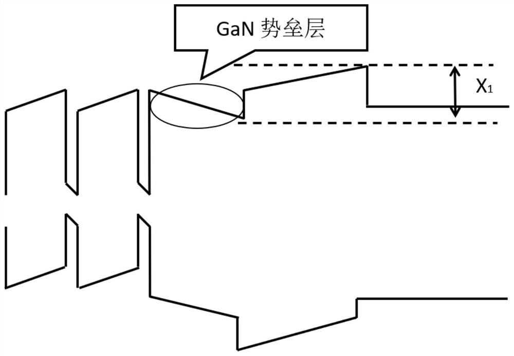
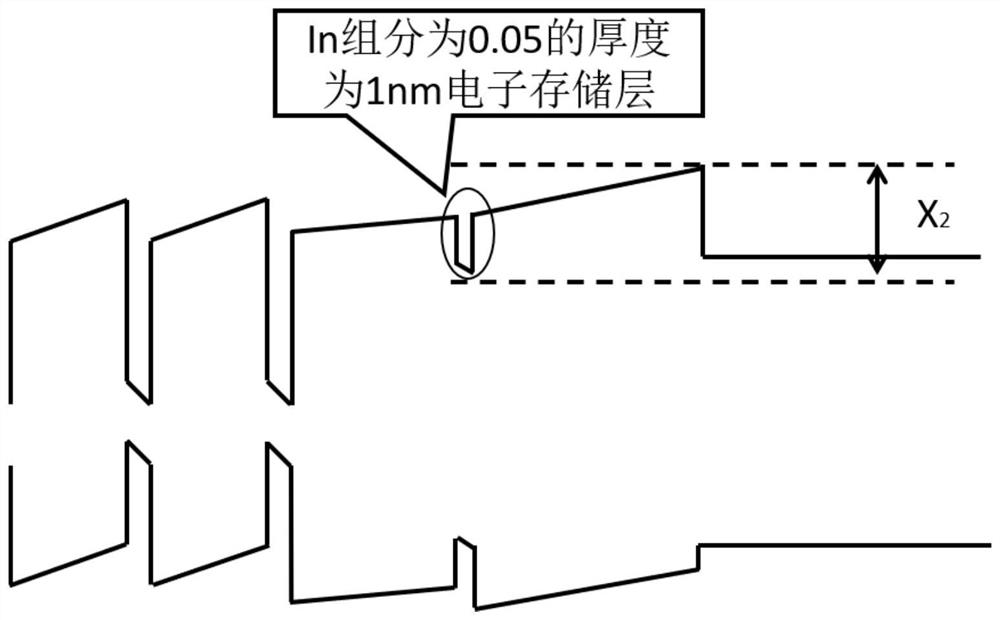
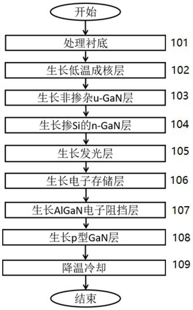
[0035] This embodiment provides an LED epitaxial structure, which sequentially includes: processing the substrate (1), growing a low-temperature nucleation layer (2), growing a non-doped low-temperature u-GaN layer (3), growing a Si-doped n-GaN layer (4), grown In y Ga 1-y N / GaN light-emitting layer (5), grown In x Ga 1-x N electron storage layer (6), growth of AlGaN electron blocking layer (7), growth of P-type GaN contact layer (8), and cooling down (9). Such as image 3 , the epitaxial layer growth method of the above structure is as follows,
[0036] Step 101, processing the substrate (1):
[0037] In a hydrogen atmosphere, the sapphire substrate is annealed at a temperature of 1100° C. to clean the surface of the substrate.
[0038] Step 102, growing a low-temperature nucleation layer GaN (2):
[0039] At 550°C, the pressure of the reaction chamber is 500 Torr, and ammonia and TMGa are introduced to grow a low-temperature nucleation layer GaN with a thickness of 30...
Embodiment 2
[0058] This embodiment provides a conventional LED epitaxial structure, the epitaxial structure sequentially includes: processing the substrate (1), growing a low-temperature nucleation layer (2), growing an undoped low-temperature u-GaN layer (3), growing a doped Si n-GaN layer (4), grown In y Ga 1-y N / GaN light-emitting layer (5), growing AlGaN electron blocking layer (6), growing P-type GaN contact layer (7), and cooling down (8). Using the conventional LED epitaxial growth method, the specific steps are:
[0059] Step 201, processing the substrate (1):
[0060] In a hydrogen atmosphere, the sapphire substrate is annealed at a temperature of 1100° C. to clean the surface of the substrate.
[0061] Step 202, growing a low-temperature nucleation layer GaN (2):
[0062] At 550°C, the pressure of the reaction chamber is 500 Torr, and ammonia and TMGa are introduced to grow a low-temperature nucleation layer GaN with a thickness of 30 nm on the sapphire substrate. To 1100°C...
PUM
| Property | Measurement | Unit |
|---|---|---|
| thickness | aaaaa | aaaaa |
| thickness | aaaaa | aaaaa |
| thickness | aaaaa | aaaaa |
Abstract
Description
Claims
Application Information
 - R&D Engineer
- R&D Manager
- IP Professional
- Industry Leading Data Capabilities
- Powerful AI technology
- Patent DNA Extraction
Browse by: Latest US Patents, China's latest patents, Technical Efficacy Thesaurus, Application Domain, Technology Topic, Popular Technical Reports.
© 2024 PatSnap. All rights reserved.Legal|Privacy policy|Modern Slavery Act Transparency Statement|Sitemap|About US| Contact US: help@patsnap.com


