5G chip processing technology

A processing technology and chip technology, applied in the field of microelectronics, can solve problems such as excessive grinding, low efficiency, and lower product quality, and achieve the effects of cost saving, high surface quality, and extended maintenance cycle

Inactive Publication Date: 2021-03-19
谢贝贝
View PDF0 Cites 0 Cited by
  • Summary
  • Abstract
  • Description
  • Claims
  • Application Information

AI Technical Summary

Problems solved by technology

[0005] In the existing gallium nitride chip manufacturing process, the surface treatment of the wafer has always been the top priority. However, in the photolithography technology, the requirements for the surface flatness of the wafer are almost strict. In the existing polishing technology, most With rotary grinding, since the linear velocity at the center of the wafer is different from that at the edge, and the linear velocity at the edge is higher, under the same pressure, it is more fully polished than the central area, forming the phenomenon of over-polishing, and also causing the wafer The round surface forms a spherical surface, which reduces the quality of the product; and most of the existing equipment can only polish one wafer at a time, and the efficiency is low

Method used


Image

  • 5G chip processing technology
  • 5G chip processing technology
  • 5G chip processing technology

Examples


Embodiment 1

[0031] A 5G chip processing technology, comprising the following steps:

[0032] Step 1: Preliminary cutting, grinding and grinding of gallium nitride wafers

[0033] Step 2: place the ground gallium nitride wafer on a precision polisher for fine polishing;

[0034] Step 3: washing the surface of the gallium nitride wafer with a cleaning agent after fine polishing, and then drying to obtain a radio frequency chip material;

[0035] The fine polishing liquid used in the fine polishing treatment includes the following components by weight: 20-30wt% mixed abrasive particles, 0.4-0.8wt% corrosive agent, 0.3-0.7wt% oxidant, 0.001-0.01wt% accelerator, water balance.

[0036] The mixed abrasive particles are composed of purified silica sol and modified boron carbide in a mass ratio of 1:1; the particle size range of the purified silica sol is 60-90 nm; the particle size range of the modified boron carbide is 100-90 nm 130nm.

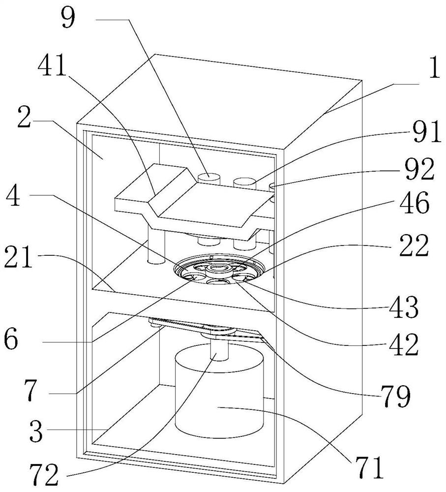
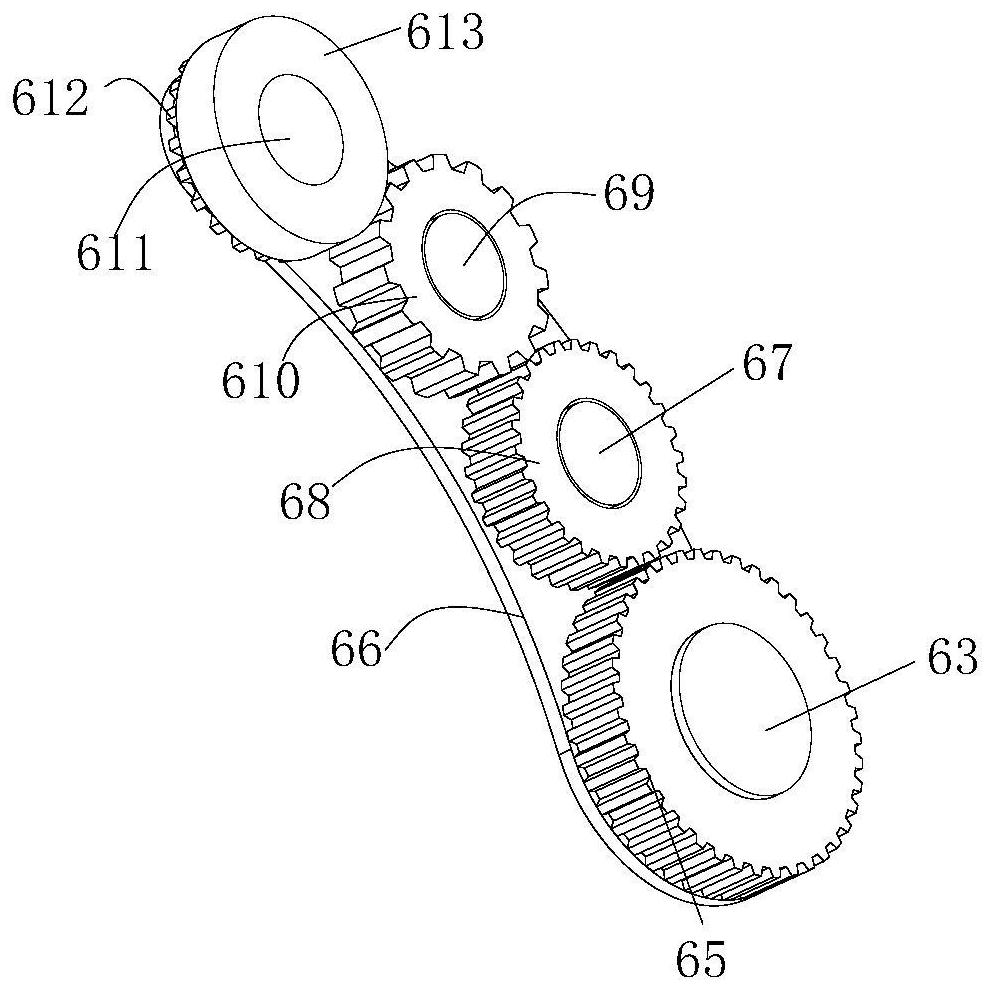
[0037] Wherein, the precision polishing apparatus in ...

Embodiment 2

[0047] A 5G chip processing technology, comprising the following steps:

[0048] Step 1: Preliminary cutting, grinding and grinding of gallium nitride wafers

[0049] Step 2: place the ground gallium nitride wafer on a precision polisher for fine polishing;

[0050] Step 3: washing the surface of the gallium nitride wafer with a cleaning agent after fine polishing, and then drying to obtain a radio frequency chip material;

[0051] The fine polishing liquid used in the fine polishing treatment includes the following components by weight: 25 wt % mixed abrasive particles, 0.6 wt % etchant, 0.5 wt % oxidant, 0.005 wt % accelerator, and water balance.

[0052] The mixed abrasive particles are composed of purified silica sol and modified boron carbide in a mass ratio of 1:1; the particle size range of the purified silica sol is 75 nm; the particle size range of the modified boron carbide is 115 nm.

[0053] The structure of the precision polishing apparatus in step 2 is the same...

Embodiment 3

[0055]A 5G chip processing technology, comprising the following steps:

[0056] Step 1: Preliminary cutting, grinding and grinding of gallium nitride wafers

[0057] Step 2: place the ground gallium nitride wafer on a precision polisher for fine polishing;

[0058] Step 3: washing the surface of the gallium nitride wafer with a cleaning agent after fine polishing, and then drying to obtain a radio frequency chip material;

[0059] The fine polishing liquid used in the fine polishing treatment includes the following components by weight: 30 wt % mixed abrasive particles, 0.8 wt % etchant, 0.7 wt % oxidant, 0.01 wt % accelerator, and water balance.

[0060] The mixed abrasive particles are composed of purified silica sol and modified boron carbide in a mass ratio of 1:1; the particle size range of the purified silica sol is 90 nm; the particle size range of the modified boron carbide is 130 nm.

[0061] The structure of the precision polishing apparatus in step 2 is the same a...


PUM

PropertyMeasurementUnit
particle diameteraaaaaaaaaa

Abstract

The invention discloses a 5G chip processing technology. The 5G chip processing technology comprises the following steps of: 1, carrying out primary cutting, grinding and lapping treatment on a gallium nitride wafer; 2, placing the lapped gallium nitride wafer on a precision polishing instrument for fine polishing treatment; and 3, washing the surfaces of the gallium nitride wafer after fine polishing with a cleaning agent, and then drying to obtain a radio-frequency chip material, wherein the precision polishing instrument in the step 2 comprises a protection box, a polishing bin, a driving bin, a bearing plate, a polishing groove, a maintaining mechanism, an ejecting device, a polishing device, a stroke device, an upper cover plate, a supercharging device arranged on the upper cover plate and a liquid feeding device arranged on the polishing bin. The flatness of the surfaces including the front surface and the back surface of the gallium nitride wafer can be improved to a new level through the precision polishing instrument, so that a 5G chip with better quality is produced, and the requirement of 5G communication is met.

Description

technical field [0001] The invention belongs to the technical field of microelectronics, and in particular relates to a 5G chip processing technology. Background technique [0002] In 5G communication technology, a large number of medium and high frequency devices are required, mainly including filters, power amplifiers, low noise amplifiers, radio frequency switches, etc.; compound semiconductor materials are the core key materials for the preparation of these devices. Compound-based semiconductor materials mainly include compound semiconductors such as gallium arsenide (GaAs), gallium nitride (GaN), and silicon carbide (SiC). Efficiency, large frequency wave processing, low latency response and other functions. Compound semiconductor materials will be widely used in 5G, Internet of Things, smart cars and other applications in the future; [0003] Compared with the mainstream silicon power devices in the market, gallium nitride has a significant order of magnitude improve...

Claims


Application Information

Patent Timeline
Patent Type & Authority Applications(China)
IPC IPC(8): B24B29/02B24B27/00B24B47/12H01L21/02C09G1/02
CPCB24B27/0023B24B27/0076B24B29/02B24B47/12C09G1/02H01L21/02013H01L21/02024
Inventor 谢贝贝
Owner 谢贝贝
Why Eureka
Try Eureka