

Semiconductor structure and forming method thereof
A technology of semiconductor and dielectric film, which is applied in the field of semiconductor structure and its formation, and can solve the problems of poor performance of magnetic tunnel junctions
- Summary
- Abstract
- Description
- Claims
- Application Information
AI Technical Summary
Problems solved by technology
Method used
Image

Examples
Embodiment Construction
[0031] As mentioned in the background, existing semiconductor structures perform poorly.
[0032] The reasons for the poor performance of the semiconductor structure will be described in detail below in conjunction with the accompanying drawings. Figure 1 to Figure 4 It is a structural schematic diagram of each step of a method for forming a semiconductor structure.
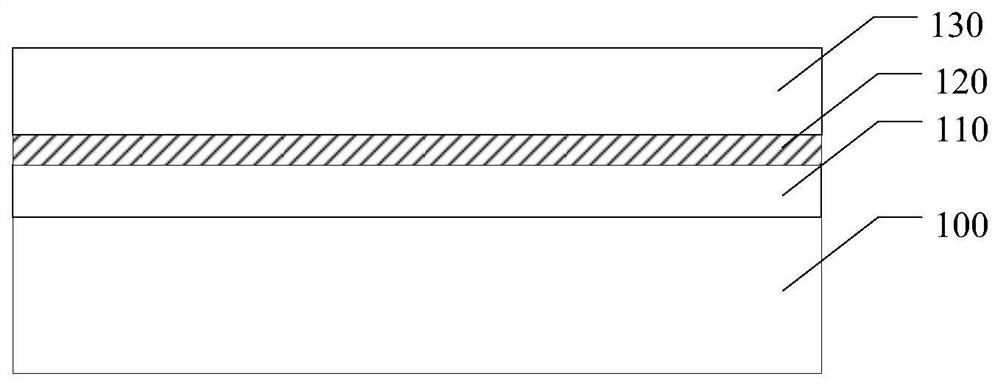
[0033] Please refer to figure 1 , a substrate 100 is provided, and the substrate 100 has a first electromagnetic film 110 , a tunnel film 120 on the surface of the first electromagnetic film 110 , and a second electromagnetic film 130 on the surface of the tunnel film 120 .
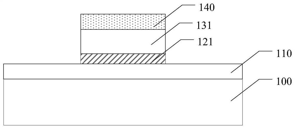
[0034] Please refer to figure 2, forming a mask layer 140 on the surface of the second electromagnetic film 130, and the mask layer 140 exposes part of the second electromagnetic film surface 130; using the mask layer 140 as a mask, etching the second The electromagnetic film 130 and the tunneling film 120 until the surface of the first...
PUM
 Abstract
Description
Claims
Application Information