Graphene transistor label-free DNA sensor and preparation method thereof

A graphene and transistor technology, which is applied in the field of biosensors to achieve the effects of low cost, high sensitivity and reduced operating voltage

Pending Publication Date: 2021-03-30
HUBEI UNIV
View PDF5 Cites 0 Cited by
  • Summary
  • Abstract
  • Description
  • Claims
  • Application Information

AI Technical Summary

Problems solved by technology

However, detection of nucleic acid molecules, especially short DNA strands, is challenging without the use of time-consuming radiolabeled assays and non-portable confocal fluorescence microscopy

Method used


Image

  • Graphene transistor label-free DNA sensor and preparation method thereof
  • Graphene transistor label-free DNA sensor and preparation method thereof
  • Graphene transistor label-free DNA sensor and preparation method thereof

Examples


preparation example Construction

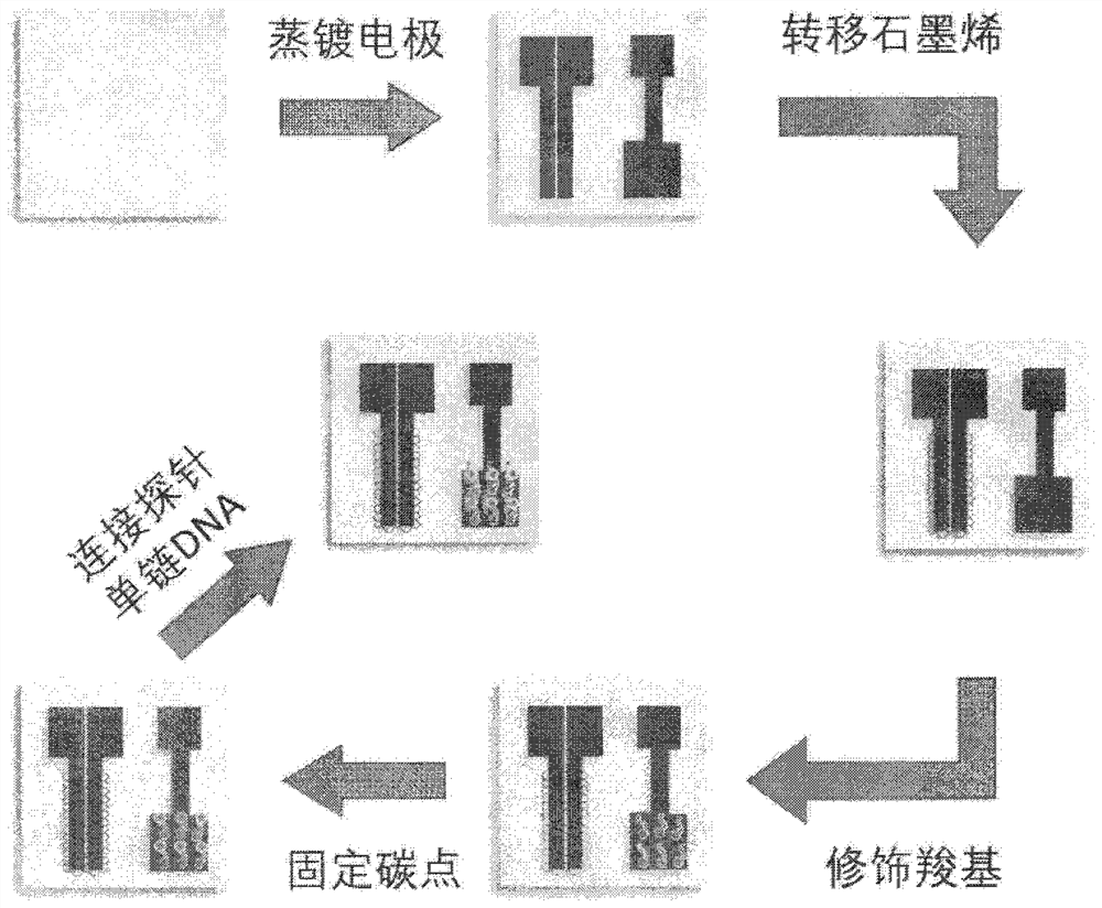
[0034] The present invention also provides the preparation method of the graphene transistor DNA sensor described in the above technical scheme, comprising the following steps:

[0035] (1) Prepare gate, source and drain on the surface of the substrate, so that there is a channel between the source and drain;

[0036] (2) Graphene is tiled on the channel between the source and the drain to obtain a graphene transistor;

[0037] (3) carbon dots are fixed on the grid surface of the graphene transistor obtained in the step (2), to obtain the graphene transistor DNA sensor.

[0038] In the present invention, gate, source and drain are prepared on the substrate surface, so that a channel exists between the source and drain. In the present invention, the preparation of the gate electrode, the source electrode and the drain electrode preferably includes: sequentially vapor-depositing a chromium layer and a gold layer on the surface of the substrate by a thermal evaporation coating m...

Embodiment 1

[0065] Thermal evaporation coating:

[0066] Cut the electronic grade glass into 12×12mm size, ultrasonically clean it with acetone, isopropanol, and ethanol for ten minutes, dry it in an oven, paste the glass piece on a mask plate of a specific shape with high-temperature glue, and weigh an appropriate amount The chromium and gold are put into the tungsten boat to prepare the vacuum thermal evaporation coating.

[0067] When evaporating, first evaporate chromium: the thickness is 8nm.

[0068] Evaporation gold layer again: the thickness is 50nm.

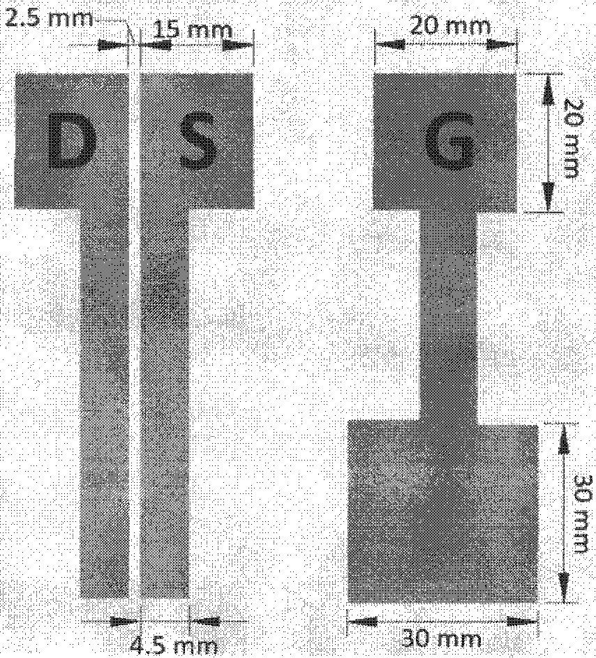
[0069] The obtained electrode shape, structure and size are as follows image 3 shown. image 3Among them, G is the gate, that is, the gate, S is the source, that is, the source, D is the drain, that is, the drain, and the 0.25mm wide channel between the source and the drain is the graphene channel after graphene is transferred.

[0070] Wet transfer of monolayer graphene:

[0071] 250 mg of methyl methacrylate (PMMA) with a mo...

Embodiment 2

[0080] Thermal evaporation coating:

[0081] Cut the electronic grade glass into 12×12mm size, ultrasonically clean it with acetone, isopropanol, and ethanol for ten minutes, dry it in an oven, paste the glass piece on a mask plate of a specific shape with high-temperature glue, and weigh an appropriate amount The chromium and gold are put into the tungsten boat to prepare the vacuum thermal evaporation coating.

[0082] When evaporating, chrome is evaporated first: the thickness is 6nm.

[0083] Evaporate a gold layer again: the thickness is 35nm.

[0084] The shape, structure and size of the obtained electrode are the same as in Example 1.

[0085] Wet transfer of monolayer graphene:

[0086] 250 mg of methyl methacrylate (PMMA) with a molecular weight of 99600 g / mol was dissolved in 5 mL of anisole, and stirred on a magnetic stirrer to obtain a clear and transparent PMMA / anisole solution with a concentration of 50 mg / mL.

[0087] Cut the single-layer copper-based graphe...


PUM

PropertyMeasurementUnit
widthaaaaaaaaaa
lengthaaaaaaaaaa
thicknessaaaaaaaaaa

Abstract

The invention provides a graphene transistor DNA sensor. The graphene transistor DNA sensor comprises a substrate, and a grid electrode, a source electrode and a drain electrode which are arranged onthe substrate, wherein a graphene channel is arranged between the source electrode and the drain electrode; and carbon dots are fixed on the surface of the grid. According to the invention, the carbondots are fixed on the surface of the gate electrode of the graphene transistor, then the single-stranded probe DNA is connected to the carbon dots, and the single-stranded DNA can be complementarilypaired with the complementary DNA in the solution, so that the interface characteristics of the double electric layers between the transistor and the sample solution are changed, the current in the graphene channel is changed, and the detection of the current change in the channel is carried out. Trace DNA in the solution can be detected; the operation voltage of the graphene transistor label-freeDNA sensor provided by the invention is lower than 1V, the lowest detection limit of DNA can reach 10-12M, and after the concentration of DNA is changed, the current of the sensor changes immediately, and the sensitivity is very high.

Description

technical field [0001] The invention relates to the technical field of biosensors, in particular to a graphene transistor label-free DNA sensor and a preparation method thereof. Background technique [0002] With the development of nanotechnology, many chemical and biological sensors or electronic devices based on nanomaterials are widely studied, and graphene is considered as a promising material in chemical and biological sensors due to its unique physical properties. [0003] Deoxyribonucleic acid (abbreviated as DNA) is a type of nucleic acid, one of the four biological macromolecules contained in biological cells. DNA carries the genetic information necessary for the synthesis of RNA and protein, and is an essential biological macromolecule for the development and normal operation of organisms. DNA diagnostics has shown great scientific and economic value in many fields. It has important application value in gene expression monitoring, clinical medicine, virus and bac...

Claims


Application Information

Patent Timeline
Patent Type & Authority Applications(China)
IPC IPC(8): G01N27/327C12Q1/6825
CPCG01N27/3275G01N27/308C12Q1/6825C12Q2563/116C12Q2565/607
Inventor 李金华范钦
Owner HUBEI UNIV
Why Eureka
Try Eureka