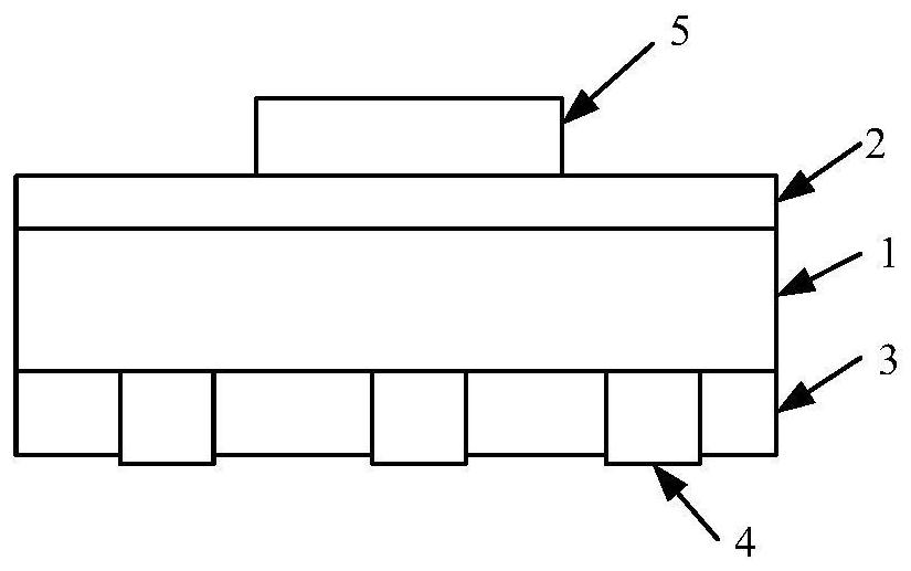
Gallium arsenide-based LED chip and preparation method thereof
An LED chip, gallium arsenide-based technology, applied in electrical components, circuits, semiconductor devices, etc., can solve the problems of low brightness of the chip, cumbersome manufacturing process, etc., and achieve the effect of increasing brightness
- Summary
- Abstract
- Description
- Claims
- Application Information
AI Technical Summary
Problems solved by technology
Method used
Image
Examples
preparation example Construction
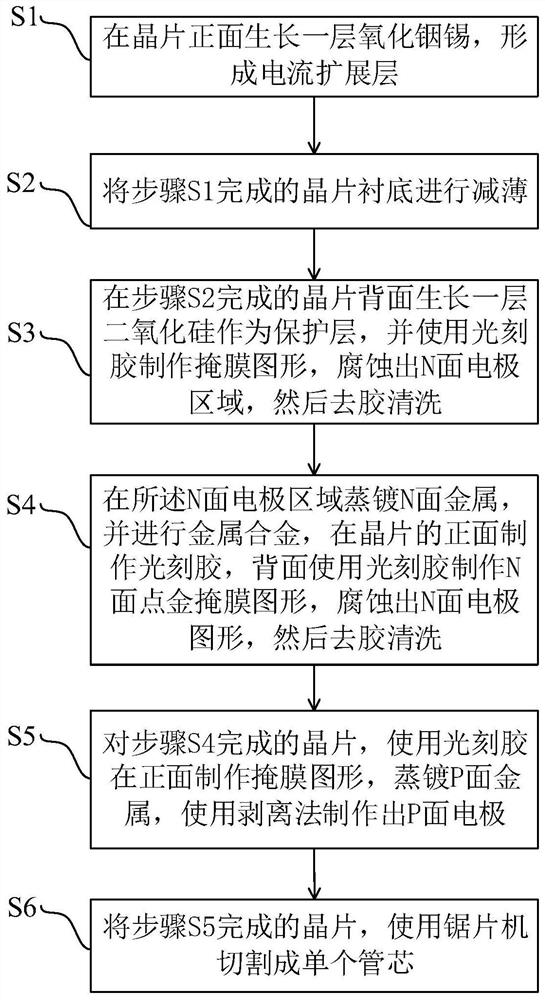
[0037] Such as figure 2 As shown, the preparation method of the LED chip specifically includes the following steps:
[0038] S1, growing a layer of indium tin oxide on the front of the wafer to form a current spreading layer;
[0039] S2, thinning the wafer substrate completed in step S1;
[0040] S3, growing a layer of silicon dioxide on the back of the wafer completed in step S2 as a protective layer, and using photoresist to make a mask pattern, etching out the N-face electrode area, and then removing the glue and cleaning;
[0041]S4, vapor-deposit N-face metal on the N-face electrode area, and perform metal alloying, make photoresist on the front side of the wafer, use photoresist on the back side to make N-face dot gold mask pattern, and corrode the N-face electrode pattern, Then remove glue and clean;
[0042] S5, for the wafer completed in step S4, use photoresist to make a mask pattern on the front side, vapor-deposit the P-side metal, and use the lift-off method ...
Embodiment 1
[0054] The thickness of the current spreading layer in step S1 is 1600 angstroms, the annealing temperature is 400° C., and the annealing time is 15 minutes; the thinned substrate in step S2 is 110 μm; the thickness of the silicon dioxide protective layer in step S3 is 2000 angstroms, and the growth temperature is 200°C; the thickness of the photoresist mask pattern in step S4 is 1 μm and the etching time is 1min; the thickness of the N surface electrode in step S4 is 3000 angstroms, and the thickness of the protective photoresist is 2 μm; the alloy temperature is 350° C., and the alloy time is 20min. The film baking temperature is 100° C., and the baking time is 20 minutes.
Embodiment 2
[0056] The thickness of the current spreading layer in step S1 is 2400 angstroms, the annealing temperature is 500° C., and the annealing time is 5 minutes; the thinned substrate in step S2 is 130 μm; the thickness of the silicon dioxide protective layer in step S3 is 4000 angstroms, and the growth temperature is 200° C.; the thickness of the photoresist mask pattern in step S4 is 3 μm, and the etching time is 3 minutes; the thickness of the N surface electrode in step S4 is 6000 angstroms, and the thickness of the protective photoresist is 3 μm; the alloy temperature is 450° C., and the alloy time is 10 minutes. The hard film baking temperature is 120°C, and the baking time is 10 minutes.
PUM
| Property | Measurement | Unit |
|---|---|---|
| temperature | aaaaa | aaaaa |
| thickness | aaaaa | aaaaa |
| thickness | aaaaa | aaaaa |
Abstract
Description
Claims
Application Information


