Preparation method of three-dimensional broken line nanowire array vertical field effect transistor

A vertical field effect and line array technology, applied in the field of microelectronics, can solve the problems of high manufacturing cost, difficulty in obtaining, and low yield, and achieve the effects of improving current load and driving capability, wide application value, and increasing integration density

Active Publication Date: 2021-04-02
NANJING UNIV
View PDF3 Cites 0 Cited by
  • Summary
  • Abstract
  • Description
  • Claims
  • Application Information

AI Technical Summary

Problems solved by technology

The nanowires prepared by the common vapor-liquid-solid (VLS) growth mode are mostly vertical random arrays, and it is difficult to directly realize reliable and low-cost positioning integration in the current planar electronic process.
Based on the top-down electron beam direct writing (EBL) technology to prepare transistor structures with nanowire diameters of 10-100 nanometers and channel lengths on the order of ten to hundreds of nanometers, the excellent characteristics of various new nanowire functional devices have been verified. , but due to factors such as high preparation

Method used


Image

  • Preparation method of three-dimensional broken line nanowire array vertical field effect transistor
  • Preparation method of three-dimensional broken line nanowire array vertical field effect transistor
  • Preparation method of three-dimensional broken line nanowire array vertical field effect transistor

Examples


Example Embodiment

[0037] Example 1

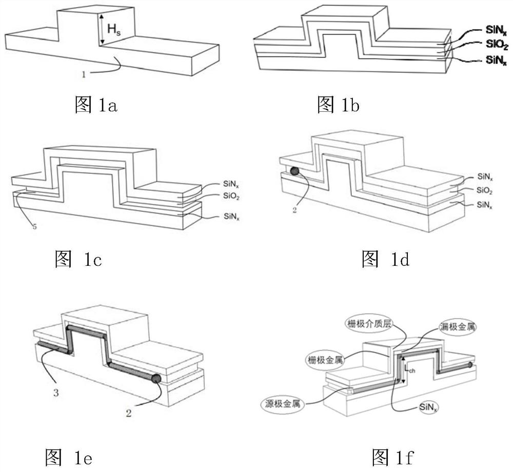
[0038] like figure 1 As shown, this embodiment provides a method for preparing a vertical gate transistor array by using a heterogeneous dielectric stack on a step to guide the growth of three-dimensional zigzag nanowires, which can be used to fabricate a vertical gate field effect transistor structure on a crystalline silicon substrate. The preparation process The following steps can be included:

[0039] 1) Use highly doped crystalline silicon as substrate 1, define the position of the guide step by photolithography, and then etch the surface of the substrate by ICP etching. The etching process uses C 4 F 8 and SF 6 Gas mixing 3:4 deep silicon etching technology to obtain vertical three-dimensional steps with a height of 200nm; such as figure 1 a shown.

[0040] 2) Alternately deposit amorphous silicon nitride-silicon oxide-silicon nitride films by plasma enhanced PECVD, the thickness of each film is 40-60-40nm respectively, and the heterogeneous die...

Example Embodiment

[0047] Example 2

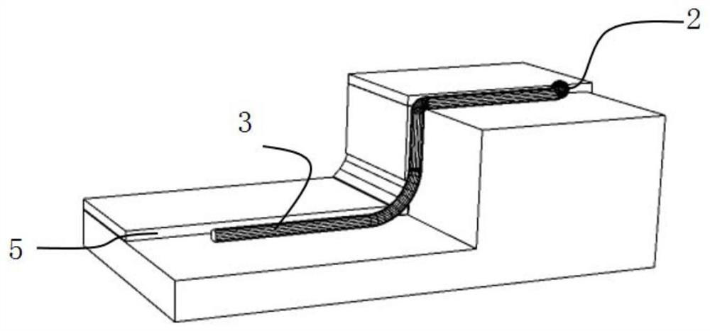
[0048] This embodiment provides a method for guiding the growth of single-layer three-dimensional zigzag nanowires by using a heterogeneous dielectric stack on a step, such as figure 2 shown, including the following steps:

[0049] 1) The shape of a single-layer three-dimensional step 5 is etched on the patterned substrate by etching technology;

[0050] 2) Deposit a homogeneous dielectric layer film on the etched substrate with three-dimensional steps, and use lithography to define the position and then etch to form a single-layer guide channel;

[0051] 3) preparing nano-scale catalytic metal particles 2 in the single-layer guiding channel;

[0052] 4) Deposit an amorphous semiconductor precursor film layer covering the desired growth nanowire on the entire surface of the structure;

[0053] 5) Raising the temperature makes the nano-scale catalytic metal particles change from solid state to liquid state in the single-layer guiding channel, the front en...

Example Embodiment

[0055] Example 3

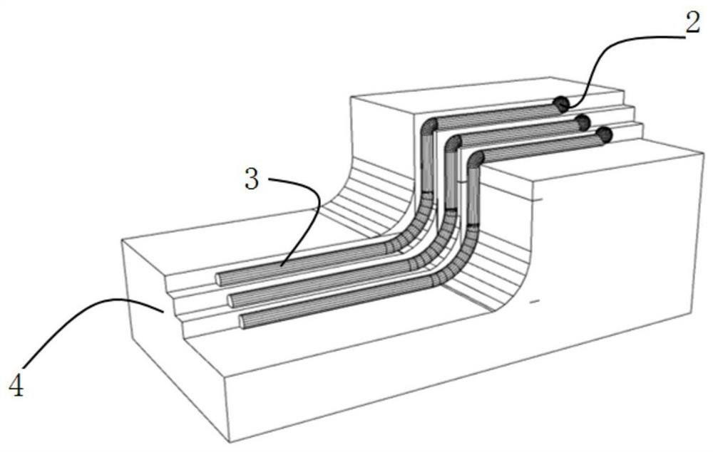
[0056] This embodiment provides a method for guiding the growth of multi-layer three-dimensional zigzag nanowires by using a heterogeneous dielectric stack on a step, such as image 3 shown, including the following steps:

[0057] 1) Using etching technology to etch the shape of multi-layer three-dimensional steps 4 on the patterned substrate;

[0058] 2) Deposit a film of a heterogeneous dielectric layer on a substrate etched with three-dimensional steps, and use lithography to define the position and then etch to form a multi-layer guide channel;

[0059] 3) preparing nano-scale catalytic metal particles 2 in the multi-layer guiding channel;

[0060] 4) Deposit an amorphous semiconductor precursor film layer covering the desired growth nanowire on the entire surface of the structure;

[0061] 5) Raising the temperature makes the nano-scale catalytic metal particles change from solid state to liquid state in the multi-layer guiding channel, the front end...


PUM

PropertyMeasurementUnit
Thicknessaaaaaaaaaa
Thicknessaaaaaaaaaa
Thicknessaaaaaaaaaa

Abstract

The invention discloses a preparation method of a three-dimensional broken line nanowire array vertical field effect transistor. The preparation method comprises the following steps: 1), etching a three-dimensional step shape on a patterned substrate by using an etching technology; 2), depositing a dielectric film layer on the substrate etched with the three-dimensional step, performing etching again to expose the heterogeneous side wall near the three-dimensional step, and constructing a guide channel on the heterogeneous side wall by using selective etching; 3), preparing nano-scale catalytic metal particles in a guide channel formed by heterogeneous side walls; 4), depositing and covering an amorphous semiconductor precursor film layer corresponding to the nanowire to be grown on the surface of the whole structure; 5), raising the temperature to convert the nanoscale catalytic metal particles into a liquid state from a solid state in the guide channel, starting to absorb the amorphous layer at the front end, and separating out the broken-line-shaped crystalline nanowire at the rear end; and 6), preparing a short-channel field effect transistor by taking the vertical part of thebroken-line-shaped crystalline nanowire as a channel region and the horizontal part as a source and drain electrode region.

Description

technical field [0001] The invention relates to a three-dimensional batch growth method of nanowires, in particular to obtain a sidewall channel by depositing a heterogeneous stack on steps for etching, and using a plane solid-liquid-solid (IPSLS) method to grow three-dimensional folded line nanowires Array method; belongs to the field of microelectronics technology. Background technique [0002] Junctionless transistors are key to developing a new generation of high-performance micro- and nanoelectronic logic, sensing, and display applications. Most of the nanowires prepared by the common gas-liquid-solid (VLS) growth mode are vertical random arrays, and it is difficult to directly achieve reliable and low-cost positioning integration in the current planar electronic process. Based on top-down electron beam writing (EBL) technology, nanowires with diameters of 10 to 100 nanometers and channel lengths in the order of 10 to 100 nanometers have been fabricated. The excellent ...

Claims


Application Information

Patent Timeline
IPC IPC(8): H01L21/336H01L21/28H01L29/06H01L29/10H01L29/423
CPCH01L29/66666H01L29/0676H01L29/1037H01L29/401H01L29/42356
Inventor 余林蔚胡瑞金王军转
Owner NANJING UNIV
Why Eureka
Try Eureka