CuO multi-phase structure material based on Cu film component and structure design and preparation method thereof
A multi-phase structure and substrate technology, applied in metal material coating process, vacuum evaporation plating, coating, etc., can solve the difficulty of precise control of oxide nanostructure, the difficulty of precise design and control of products, and the work of oxide growth Less problems, to achieve the effect of enhanced physical and chemical properties, enhanced physical and chemical properties, no need for catalysts
- Summary
- Abstract
- Description
- Claims
- Application Information
AI Technical Summary
Problems solved by technology
Method used
Image

Examples
Embodiment 1
[0054] Preparation of Cu / C composite film on the Si base of embodiment 1
[0055] The Cu / C composite film was deposited on the N-type Si(100) substrate by the DC / RF co-sputtering method, and the specific preparation process was as follows:
[0056] (1) The N-type Si substrate was ultrasonically cleaned with acetone and ethanol for 15 minutes, dried and stuck to the sample holder, and then put into the sample position in the vacuum chamber.
[0057] (2) Polish the target with sandpaper to remove impurities such as oxides on the surface of the Cu target and the C target.
[0058] (3) Set the following parameters: the background vacuum is 2×10 -4 Pa, argon atmosphere, sputtering pressure 2Pa, co-sputtering of Cu target and C target, in which, the power of DC sputtering Cu target is 150w, the power of RF sputtering C target is 150w, and the co-sputtering time is 30min , Cu / C composite film was obtained by deposition at room temperature.
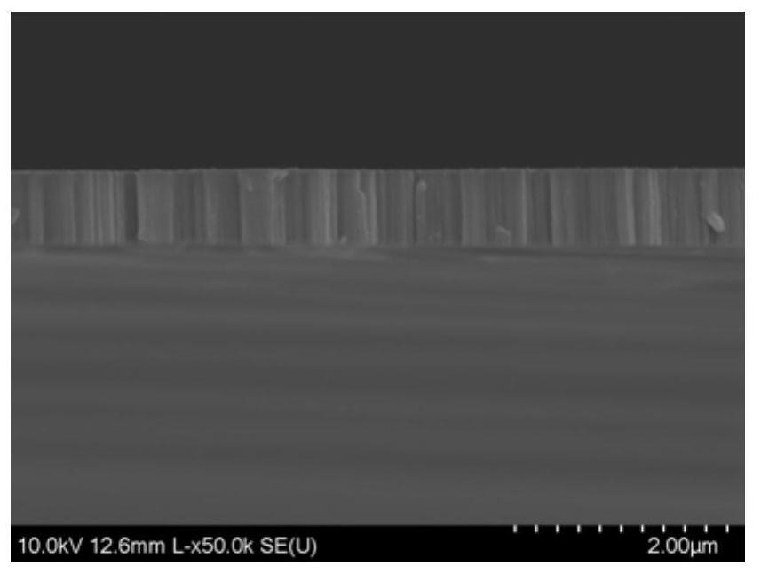
[0059] The cross-sectional scanning ele...
Embodiment 2
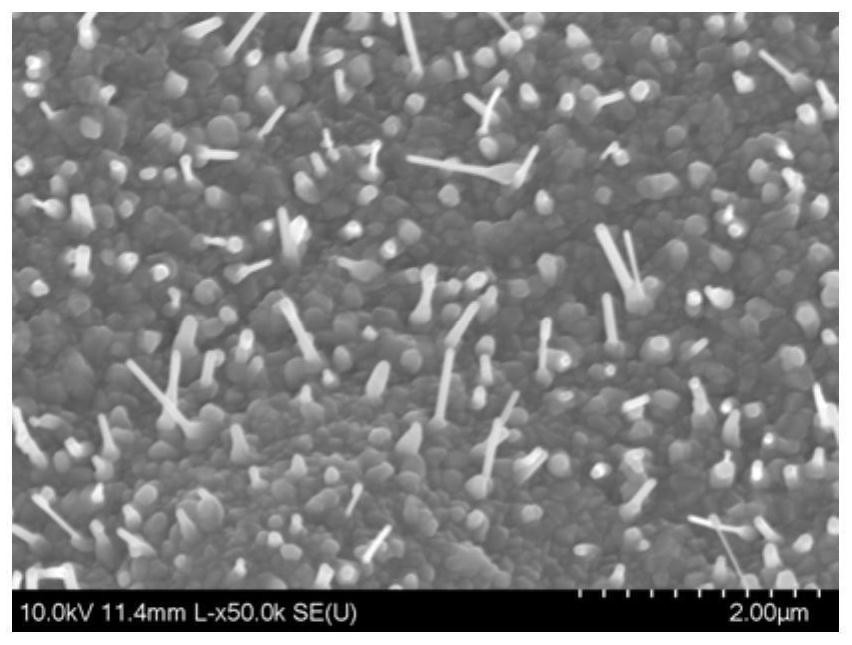
[0060] Example 2 Preparation of CuO nanorods by oxidation of Cu / C composite film on Ni foam
[0061] In this example, CuO nanorods were prepared by thermally oxidizing a Cu / C composite film on foamed Ni. The specific process is as follows:
[0062] (1) Preparation of Cu / C composite film on Ni foam
[0063] Referring to the method described in Example 1, a Cu / C composite film was prepared on a foamed Ni substrate. The only difference from Example 1 is that the substrate material is different. In this embodiment, foamed Ni is used as the substrate.
[0064] (2) Preparation of CuO nanorods by thermal oxidation of Cu / C composite film on Ni foam
[0065] CuO nanorods were prepared by heating the Cu / C composite film grown on foamed Ni by electric field-assisted thermal oxidation method, wherein the thermal oxidation temperature was 400°C, the time was 8h, the air atmosphere, and the electric field strength was 16667Vm -1 , the direction of the electric field is perpendicular to th...
Embodiment 3
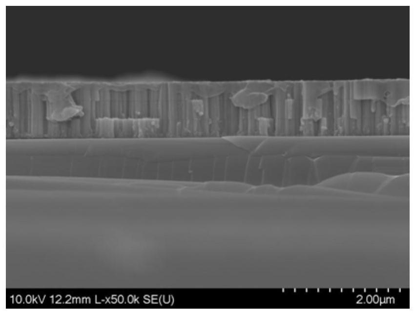
[0067] Example 3 Preparation of Cu / C multilayer film on Si base
[0068] This embodiment provides a method for preparing a Cu / C multilayer film on a Si base, and the specific steps are as follows:
[0069] (1) The N-type Si substrate was ultrasonically cleaned with acetone and ethanol for 15 minutes, dried and stuck to the sample holder, and then put into the sample position in the vacuum chamber.
[0070] (2) Polish the target with sandpaper to remove impurities such as oxides on the surface of the Cu target and the C target.
[0071] (3) Set the following parameters: the background vacuum is 2×10 -4 Pa, argon atmosphere, sputtering pressure is 2Pa; first, a Cu layer is deposited on the Si substrate by DC sputtering a Cu target with a power of 150w, and then a C layer is formed on the Cu layer by a RF sputtering C target with a power of 150w, Then use 150w DC sputtering Cu target to deposit on C layer to form Cu layer, then use 150w power RF sputtering C target to form C la...
PUM
 Abstract
Description
Claims
Application Information
 - R&D
- Intellectual Property
- Life Sciences
- Materials
- Tech Scout
- Unparalleled Data Quality
- Higher Quality Content
- 60% Fewer Hallucinations
Browse by: Latest US Patents, China's latest patents, Technical Efficacy Thesaurus, Application Domain, Technology Topic, Popular Technical Reports.
© 2025 PatSnap. All rights reserved.Legal|Privacy policy|Modern Slavery Act Transparency Statement|Sitemap|About US| Contact US: help@patsnap.com