Trench type silicon carbide reverse blocking MOSFET device and production method thereof

A silicon carbide, trench-type technology, applied in semiconductor/solid-state device manufacturing, semiconductor devices, electrical components, etc.

Active Publication Date: 2021-04-20
UNIV OF ELECTRONICS SCI & TECH OF CHINA
View PDF6 Cites 4 Cited by
  • Summary
  • Abstract
  • Description
  • Claims
  • Application Information

AI Technical Summary

Problems solved by technology

[0005] The purpose of the present invention is to solve the problem of how to make the trench silicon carbide MOS

Method used


Image

  • Trench type silicon carbide reverse blocking MOSFET device and production method thereof
  • Trench type silicon carbide reverse blocking MOSFET device and production method thereof
  • Trench type silicon carbide reverse blocking MOSFET device and production method thereof

Examples


Embodiment 1

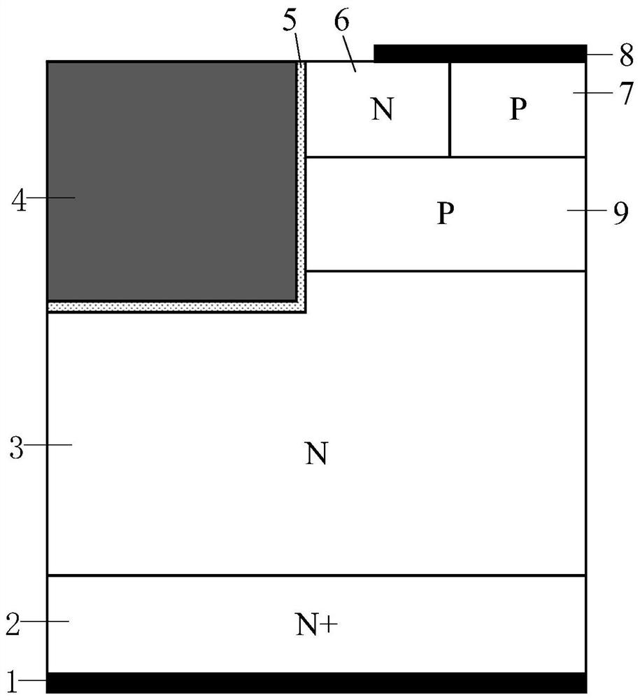
[0087] A trench type silicon carbide reverse resistance MOSFET, its semi-cellular structure is as follows figure 2 As shown, it includes: a back drain metal 1, a second N-type silicon carbide buffer layer 21, and an N-type silicon carbide epitaxial layer 3, which are stacked sequentially from bottom to top.

[0088] The gate 4 and the first N-type silicon carbide buffer layer 10 are arranged above the N-type silicon carbide epitaxial layer 3, the first N-type silicon carbide buffer layer 10 is located on the right side of the gate 4, and the first N-type silicon carbide buffer layer 10 is arranged above the first N-type silicon carbide buffer layer 10 A P-type silicon carbide base region 9, an N-type silicon carbide source region 6 and a P-type silicon carbide source region 7 are arranged above the P-type silicon carbide base region 9; the N-type silicon carbide source region 6 and the P-type silicon carbide The silicon source region 7 is connected left and right; the source ...

Embodiment 2

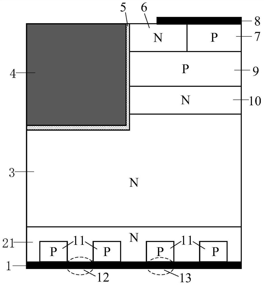
[0103] A trench type silicon carbide reverse resistance MOSFET, its semi-cellular structure is as follows image 3 As shown, the difference between this embodiment and Embodiment 1 is that: the second N-type silicon carbide buffer layer 21 has a non-adjacent P-type floating region 17; the bottom of the P-type floating region 17 is not connected to the back drain. Contact is formed between the pole metals 1, that is, the P-type floating region 17 is completely floating in the second N-type silicon carbide buffer layer 21; a Schottke is formed between the second N-type silicon carbide buffer layer 21 and the back drain metal 1. base contact.

[0104] Preferably, all silicon carbide materials are replaced with gallium nitride, gallium oxide, boron nitride, and silicon materials.

[0105] This embodiment also provides a method for preparing the trench-type silicon carbide reverse resistance MOSFET device, including the following preparation steps:

[0106] Step 1: using an epita...

Embodiment 3

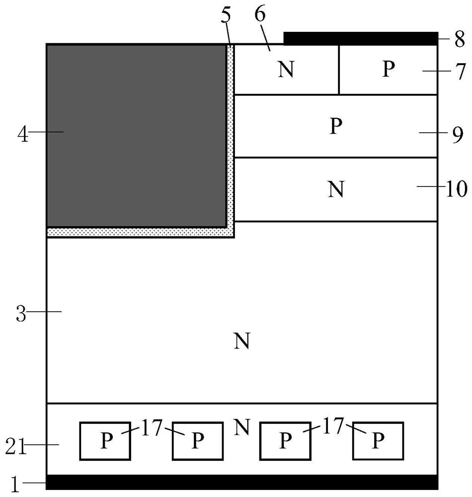
[0116] A kind of derivation structure of embodiment 1, its semicellular structure such as Figure 4 As shown, the difference between this embodiment and Embodiment 1 is that: a P-type buried layer 14 is provided at the bottom of the gate dielectric layer 5 . The specific principle is: since silicon carbide has a higher critical breakdown electric field than silicon, the higher critical breakdown electric field causes the electric field in the gate dielectric layer of the silicon carbide MOSFET device to be much larger than that of the silicon-based MOSFET gate when it breaks down. The electric field in the dielectric layer reduces the reliability of the gate dielectric layer. The P-type buried layer 14 introduced in this embodiment can effectively reduce the magnitude of the electric field in the gate dielectric layer at the bottom corner of the trench and improve the forward withstand voltage capability.


PUM


Abstract

The invention belongs to the technical field of power semiconductor devices, and particularly relates to a trench type silicon carbide reverse blocking MOSFET device and a production method thereof. Compared with a traditional trench type silicon carbide MOSFET, by using the device of the invention, an N-type silicon carbide substrate is removed, a first N-type silicon carbide buffer layer is introduced to one side of a device source region, a second N-type silicon carbide buffer layer is introduced to one side of a device drain region, and a junction Schottky barrier diode structure is introduced to one side of the device drain region. The device structure can enable the trench type silicon carbide MOSFET to obtain a large forward and reverse symmetrical withstand voltage and to have small forward conduction voltage drop at the same time. In addition, in order to further solve the reliability problem of a gate oxide layer of the device and the problem of a large gate-drain capacitance, several corresponding derivative structures are provided.

Description

technical field [0001] The invention belongs to the technical field of power semiconductor devices, and in particular relates to a trench type silicon carbide reverse resistance MOSFET device and a preparation method thereof. Background technique [0002] The inverter is a device that converts direct current into alternating current. It has a wide range of application scenarios, such as photovoltaic inverters, uninterruptible power supplies, rail transit and trolleybuses, and frequency converters. Multilevel inverters have excellent characteristics such as low loss, low noise, and output waveforms close to sine waves, so their application scenarios are broader. Matrix inverter is a new type of power converter, which can directly realize AC-AC conversion. Compared with the traditional AC-DC-AC frequency conversion method, the matrix inverter does not require DC capacitors for intermediate energy storage, which improves the reliability of the entire system and reduces costs. ...

Claims


Application Information

Patent Timeline
IPC IPC(8): H01L29/78H01L29/08H01L29/06H01L21/336
CPCY02B70/10
Inventor 张金平王鹏蛟兰逸飞刘竞秀张波
Owner UNIV OF ELECTRONICS SCI & TECH OF CHINA
Why Eureka
Try Eureka