Processing method of non-magnetic electric heater based on MEMS technology

A processing method and heater technology, applied in the process of producing decorative surface effects, microstructure technology, piezoelectric/electrostrictive/magnetostrictive devices, etc., to solve the problem of electrical insulation and reduce the effect of magnetic field

Inactive Publication Date: 2021-04-23
BEIJING AUTOMATION CONTROL EQUIP INST
View PDF8 Cites 1 Cited by
  • Summary
  • Abstract
  • Description
  • Claims
  • Application Information

AI Technical Summary

Problems solved by technology

[0006] The invention proposes a method for processing a non-magnetic electric heater based on MEMS technology, which can effectively offset the magnetic field generated during the electrification process and solve the problem of electrical insulation between double-layer metals

Method used


Image

  • Processing method of non-magnetic electric heater based on MEMS technology

Examples


Embodiment 1

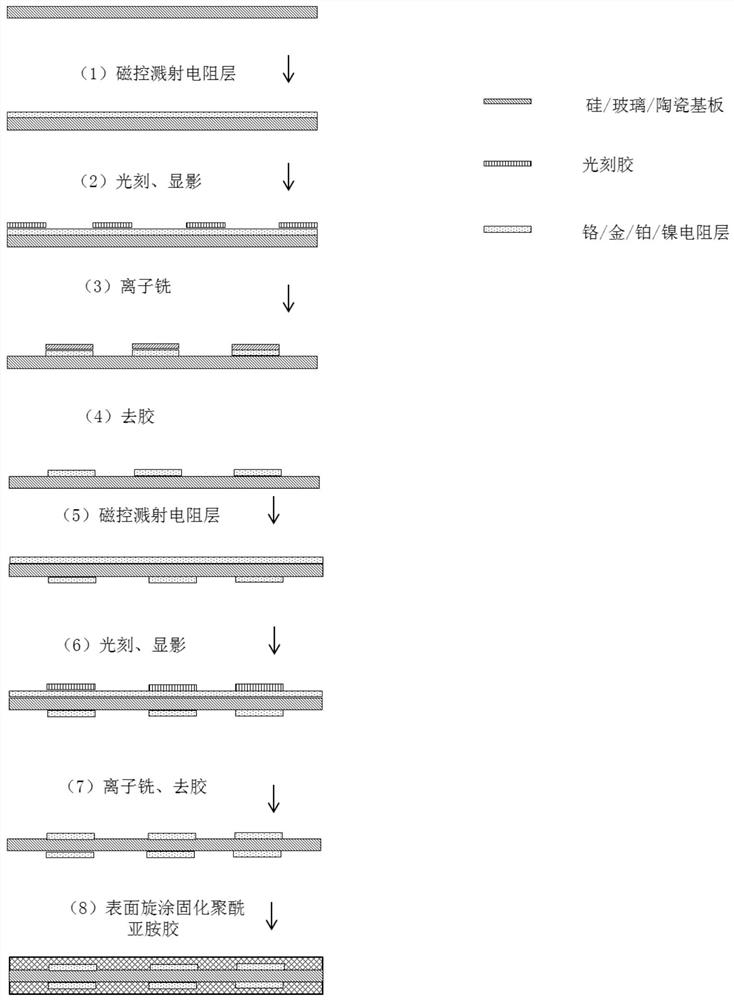
[0031] The first step is to process a resistance layer on the surface of a single crystal silicon wafer or ceramic or glass substrate: Magnetron sputtering of chromium / gold resistance layer on the surface of a single crystal silicon wafer or ceramic or glass, in which metal chromium is sputtered as an adhesion layer, gold as a resistive layer;

[0032] The second step, photolithography and development: pattern the surface of the substrate after sputtering the resistance layer, spin-coat a 5-micron-thick positive photoresist by using a positive resist process and perform a pre-baking process. Expose in the engraving machine, and finally develop and pattern in the developer;

[0033] The third step, ion milling: the patterned substrate is placed in an ion etching machine for ion milling process. Since the unpatterned area of ​​the surface after removing the photoresist still has a chromium / gold seed layer, it is necessary to use a dry The excess metal layer is removed by French...

Embodiment 2

[0037] The difference between this embodiment and embodiment 1 is that in the first step, the chromium with excessive adhesion function in the resistance layer is replaced by metal titanium with higher adhesion function, the thickness is 30-80nm, and the thickness of the gold conductive layer is 100- 500nm; in the second step, a positive photoresist with a thickness of 10 microns and a line width of 20-300um is spin-coated by the positive resist process and pre-baked; in the third step, the resistive device layer is patterned by the ion milling process.

Embodiment 3

[0039] The difference between this embodiment and embodiment 1 is that in the first step, the chromium with excessive adhesion function in the resistance layer is replaced by metal titanium with higher adhesion function, the thickness is 30-80nm, and gold is replaced by platinum as the resistance layer. The thickness is 100-3000nm; in the second step, a positive photoresist with a thickness of 10 microns and a line width of 20-300um is spin-coated in the second step and pre-baked; graphics.


PUM

PropertyMeasurementUnit
thicknessaaaaaaaaaa
thicknessaaaaaaaaaa
thicknessaaaaaaaaaa

Abstract

The invention discloses a processing method of a non-magnetic electric heater based on an MEMS technology. The processing method comprises the following steps: processing a resistance layer on the surface of a monocrystalline silicon wafer or a ceramic and glass substrate; and performing photoetching, developing, ion milling and spin coating of a photoetching type polyimide film; and repeating the process on the back surface of the processed substrate surface to prepare the back surface metal layer and process the surface insulating layer. The magnetic field generated in the electrifying process can be effectively counteracted, and the problem of electric insulation between double layers of metal is solved.

Description

technical field [0001] The invention belongs to the technical field of micro-electro-mechanical systems, and in particular relates to a micro-heater processing method for MEMS devices. Background technique [0002] Micro heaters are widely used in various applications, such as microfluidic chips, batteries, computer equipment, medical equipment, and optical equipment. The non-magnetic micro-heater has a wide range of application requirements in the field of quantum sensing, such as the temperature control of the quantum sensor light source, the temperature control of the atomic gas chamber, and other occasions. The non-magnetic micro-heater generally includes a heat-resistant insulating base layer, a double-layer heating wire, an insulating heat-resistant material between the double-layer heating wires, a surface insulating material, and the like. [0003] Polyimide polymers are generally used as substrates for heaters due to their excellent point insulation properties and ...

Claims


Application Information

Patent Timeline
Patent Type & Authority Applications(China)
IPC IPC(8): B81B7/02B81C1/00
CPCB81B7/02B81C1/00023B81C1/00206B81C1/00349B81C1/0069B81B2201/00
Inventor 秦杰谢耀万双爱
Owner BEIJING AUTOMATION CONTROL EQUIP INST
Why Eureka
Try Eureka