Organic semiconductor film and preparation method thereof

A technology of organic semiconductor and thin film, which is applied in the field of organic semiconductor thin film and its preparation, can solve the problems such as the decrease of fluorescence intensity, and achieve the effects of avoiding contradictions, improving solution processing performance, and high stability

Active Publication Date: 2021-04-30
SHANGHAI BEEN SEMICON TECH CO LTD
View PDF9 Cites 1 Cited by
  • Summary
  • Abstract
  • Description
  • Claims
  • Application Information

AI Technical Summary

Problems solved by technology

However, the reduction of quantum dot spacing will lead to enhanced fluorescence resonance energy transfer (FRET) between neighboring quantum dots, which is also an important reason for the decrease of fluorescence intensity.

Method used


Image

  • Organic semiconductor film and preparation method thereof
  • Organic semiconductor film and preparation method thereof
  • Organic semiconductor film and preparation method thereof

Examples


preparation example Construction

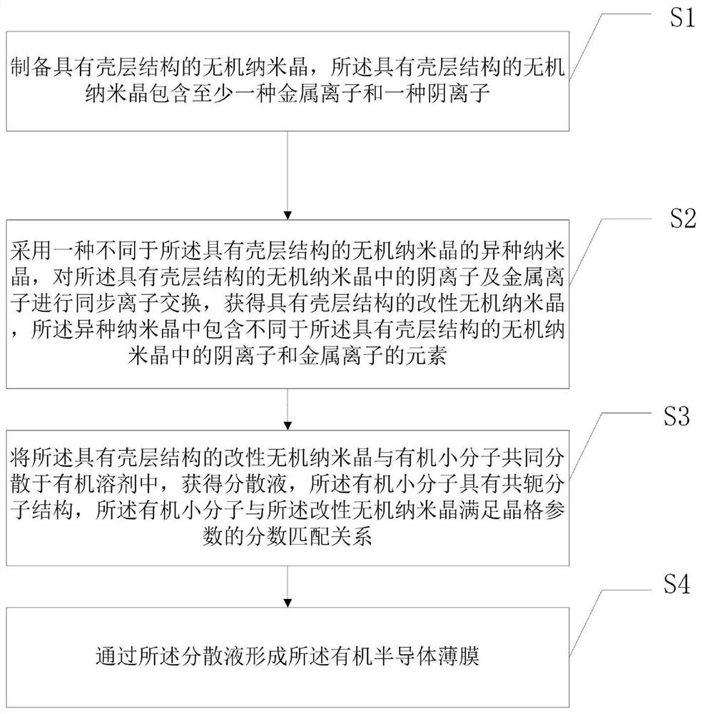
[0043] see figure 1 , the invention provides a kind of preparation method of organic semiconductor thin film, it comprises the following steps at least:

[0044] S1. Prepare an inorganic nanocrystal with a shell structure, the inorganic nanocrystal with a shell structure comprising at least one metal ion and one anion;

[0045] S2. Using a heterogeneous nanocrystal different from the inorganic nanocrystal with a shell structure, performing synchronous ion exchange on the anions and metal ions in the inorganic nanocrystal with a shell structure to obtain a shell structure Modified inorganic nanocrystals, the heterogeneous nanocrystals contain elements different from the anions and metal ions in the inorganic nanocrystals with a shell structure;

[0046] S3. Disperse the modified inorganic nanocrystals with a shell structure and organic small molecules in an organic solvent to obtain a dispersion liquid. The organic small molecules have a conjugated molecular structure, and the...

Embodiment 1

[0065] Please also refer to Figure 5 , using in situ mercaptosilane passivation method to prepare in situ mercapto nanocrystals (InMP-CsPbBr 3 ), that is, in the preparation of CsPbBr using the hot injection method 3 In the process of nanocrystallization, 3-mercaptopropyltrimethoxysilane (MPTMS) was added as a ligand in the precursor solution. Films were prepared on glass substrates by drop coating, and the XRD results of the nanocrystalline films obtained by 2θ scanning were as follows: Figure 5 shown, showing CsPbBr 3 There is lattice continuity between the cubic phase lattice of silicon oxide and the hexagonal phase lattice of silicon oxide, and the specific performance has the following characteristics: (1) (200) interplanar spacing d of the cubic phase 200 d with hexagon 011 Similar, corresponding to the 2θ diffraction peaks at ~30.6° and ~30.4° respectively; (2) Referring to the column height of the PDF card, the cubic phase CsPbBr 3 Compared with the (211) diffra...

Embodiment 2

[0067] see Figure 6 to Figure 10 , different from Example 1, the preparation method of the present invention can also adopt the method of ligand exchange to prepare the mercapto-silane-passivated mercapto-exchanged nanocrystals (ExMP-CsPbBr 3 ), the formed nanocrystalline powder XRD with a shell structure shows Image 6 shown. This method is used in the preparation of CsPbBr by hot injection 3 In the process of nanocrystals, MPTMS was not added to the precursor solution; the resulting CsPbBr 3 The heptane dispersion of nanocrystals was mixed with MPTMS at a certain volume ratio at room temperature and stirred for 12 hours to obtain ExMP-CsPbBr 3 Nanocrystalline. Compared to the control sample without ligand exchange, the cubic phase CsPbBr 3 The (200) diffraction peak shifts slightly to the small angle direction, and the crystallinity decreases to a certain extent, which is the result of the stress exerted by the silica shell on the perovskite cubic lattice. see Figur...


PUM


Abstract

The invention discloses an organic semiconductor film and a preparation method thereof. The preparation method at least comprises the following steps: preparing inorganic nanocrystalline with a shell structure; carrying out synchronous ion exchange on anions and metal ions in the inorganic nanocrystalline with the shell structure to obtain modified inorganic nanocrystalline with the shell structure and a relatively stable structure; jointly dispersing the modified inorganic nanocrystalline with the shell structure and conjugated organic small molecules into an organic solvent to obtain dispersion liquid; and forming the organic semiconductor thin film through the dispersion liquid. By independently regulating and controlling the photoelectric property and the crystal morphology of the organic semiconductor film material, the organic semiconductor film material with excellent optical property and carrier transport property is obtained.

Description

technical field [0001] The invention belongs to the field of semiconductor material preparation, in particular to an organic semiconductor thin film and a preparation method thereof. Background technique [0002] In high-performance semiconductor devices, the semiconductor functional layer is usually required to be a single crystal morphology, and the defect density at the interface is very low. The existing semiconductor technology is mainly based on the vapor phase epitaxial growth technology of two-dimensional planar structure to form high-quality inorganic semiconductor single crystal material. This method can ensure that the interface trap density is small enough. However, the vapor phase epitaxy growth process requires the substrate to be a high-quality single crystal, so it cannot be applied to low-cost transparent amorphous substrates such as glass and plastic. The special out-of-plane orientation polycrystalline film can be formed on the amorphous glass substrate b...

Claims


Application Information

Patent Timeline
Patent Type & Authority Applications(China)
IPC IPC(8): C09K11/02C09K11/66
CPCC09K11/025C09K11/665Y02E10/549
Inventor 王向华
Owner SHANGHAI BEEN SEMICON TECH CO LTD
Why Eureka
Try Eureka