A preparation method of high-power semiconductor optical amplifier gain medium

A gain medium and optical amplifier technology, applied in the field of optoelectronics, can solve problems such as insufficient gain, and achieve the effects of wide spectral gain, slow film growth rate, and high power

Active Publication Date: 2022-04-29
苏州零维量点光电科技有限公司
View PDF0 Cites 0 Cited by
  • Summary
  • Abstract
  • Description
  • Claims
  • Application Information

AI Technical Summary

Problems solved by technology

However, quantum dot materials have the disadvantage of insufficient gain compared with traditional quantum well materials

Method used


Image

  • A preparation method of high-power semiconductor optical amplifier gain medium
  • A preparation method of high-power semiconductor optical amplifier gain medium
  • A preparation method of high-power semiconductor optical amplifier gain medium

Examples


Embodiment Construction

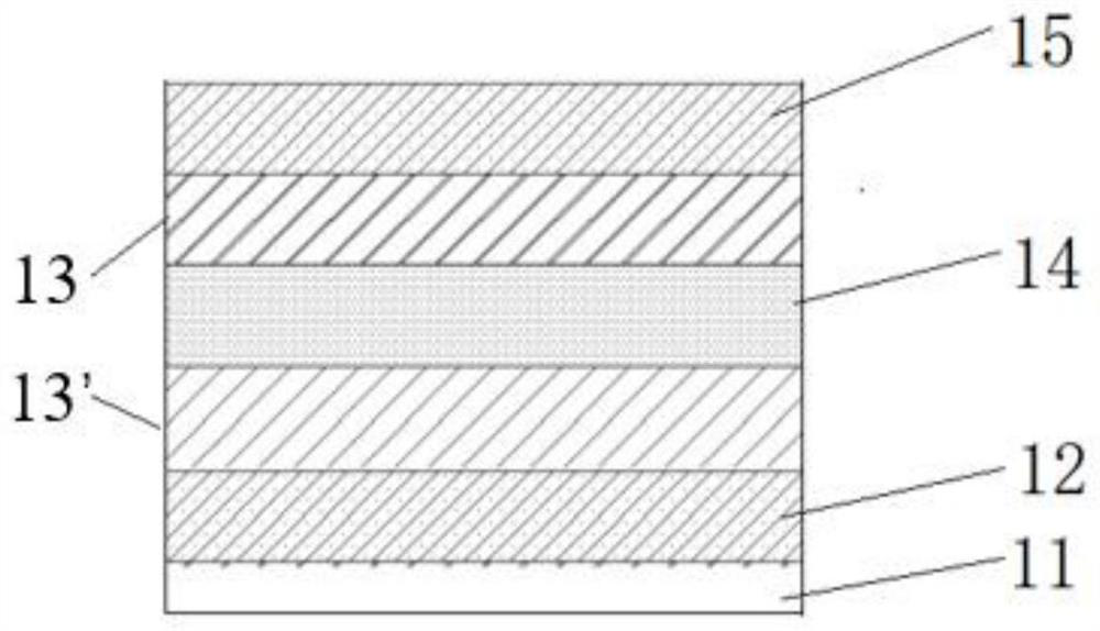
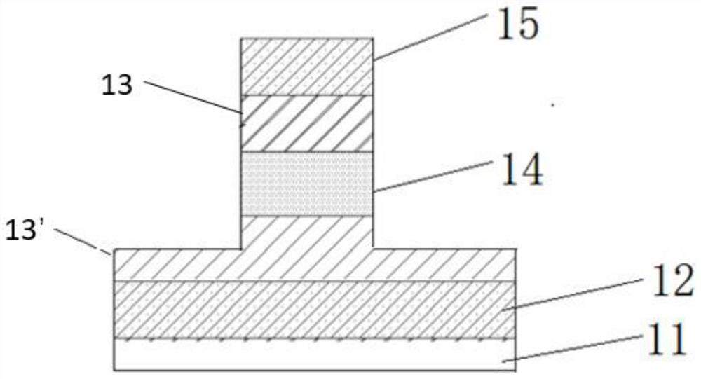
[0028] It should be noted that, in the case of no conflict, the embodiments in the present application and the features in the embodiments can be combined with each other.

[0029] In the description of the present application, it should be understood that the terms "center", "longitudinal", "transverse", "upper", "lower", "front", "rear", "left", "right", " The orientation or positional relationship indicated by "vertical", "horizontal", "top", "bottom", "inner", "outer" etc. is based on the orientation or positional relationship shown in the drawings, and is only for the convenience of describing the present application and Simplified descriptions do not indicate or imply that the device or element referred to must have a specific orientation, be constructed and operate in a specific orientation, and thus should not be construed as limiting the scope of protection of the present application. In addition, the terms "first", "second" and the like are used for descriptive purpo...


PUM

PropertyMeasurementUnit
diameteraaaaaaaaaa

Abstract

A method for preparing a high-power semiconductor optical amplifier gain medium, comprising: providing a substrate; sequentially growing a buffer layer, an n-electrode layer, a lower confinement layer, an active layer, an upper confinement layer, and a p-electrode layer on the substrate; depositing a p The p-type metal is used to make the p-type electrode; the gain medium series pattern is made; the ridge waveguide structure is etched to the n-electrode layer to form the gain medium; the n-type metal is deposited to make the electrode. In order to better control the optical field, a deep etching process is used to etch the waveguide structure through the active region (layer), such as etching through the upper confinement layer and the active layer, and etching to part of the lower confinement layer. Among them, molecular beam epitaxy is an epitaxial film-forming method, which is a method of growing thin films layer by layer along the crystal axis direction of the substrate material under suitable substrates and suitable conditions. The temperature of the substrate used is low, the growth rate of the film layer is slow, the beam intensity is easy to control precisely, and the film composition and doping concentration can be adjusted rapidly with the change of the source.

Description

【Technical field】 [0001] The invention relates to the field of optoelectronics, in particular to a method for preparing a high-power semiconductor optical amplifier gain medium. 【Background technique】 [0002] An optical amplifier is a subsystem product that can amplify optical signals in an optical fiber communication system. The principle of the optical amplifier is basically based on the stimulated radiation of laser, and the amplification effect is realized by converting the energy of the pump light into the energy of the signal light. The successful development and industrialization of optical amplifiers is a very important achievement in optical fiber communication technology, which greatly promotes the development of optical multiplexing technology, optical soliton communication and all-optical network. There are two main types of optical amplifiers, semiconductor optical amplifiers and optical fiber amplifiers. A semiconductor amplifier generally refers to a travel...

Claims


Application Information

Patent Timeline
Patent Type & Authority Patents(China)
IPC IPC(8): H01S5/22H01S5/50H01S5/34
CPCH01S5/22H01S5/5027H01S5/3412H01S2304/02
Inventor 陈嘉健陈亦凡魏玲
Owner 苏州零维量点光电科技有限公司
Why Eureka
Try Eureka