Electromagnetic field coupling high aspect ratio silicon substrate etching method

A high aspect ratio, electromagnetic field technology, applied in the manufacture of circuits, electrical components, semiconductor/solid state devices, etc., can solve the problems of uneven surface quality of formed structures, lack of electromagnetic field coupling interaction, etc., to avoid lattice defects, avoid Effects of mechanical stress and porosity reduction

Pending Publication Date: 2021-05-04
HANGZHOU DIANZI UNIV
View PDF0 Cites 1 Cited by
  • Summary
  • Abstract
  • Description
  • Claims
  • Application Information

AI Technical Summary

Problems solved by technology

However, the current magnetic field-assisted metal chemical etching method lacks the research of electromagnetic field coupling interaction, and the surface quality is still random during the structure forming process, resulting in uneven surface quality of the formed structure.

Method used


Image

  • Electromagnetic field coupling high aspect ratio silicon substrate etching method
  • Electromagnetic field coupling high aspect ratio silicon substrate etching method
  • Electromagnetic field coupling high aspect ratio silicon substrate etching method

Examples


Embodiment Construction

[0025] Embodiments of the present invention will be described in detail below in conjunction with the accompanying drawings.

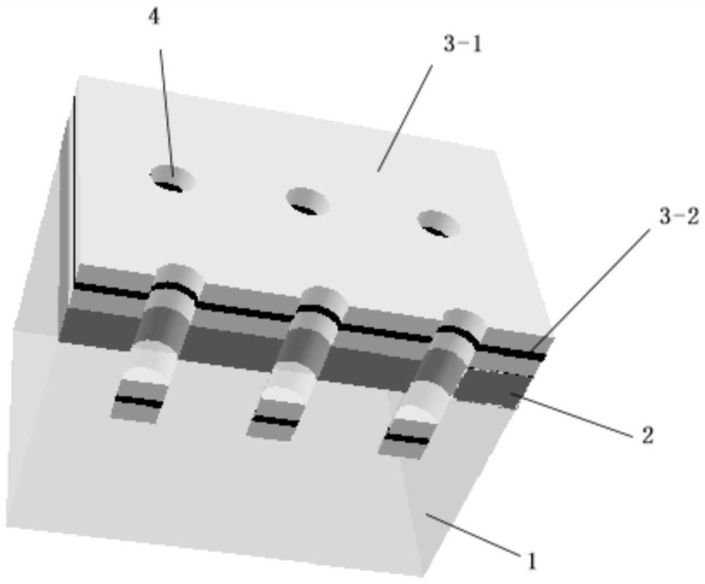
[0026] Such as Figure 1-4 As shown, the electromagnetic field coupled high aspect ratio etching method for silicon substrates includes the following steps:

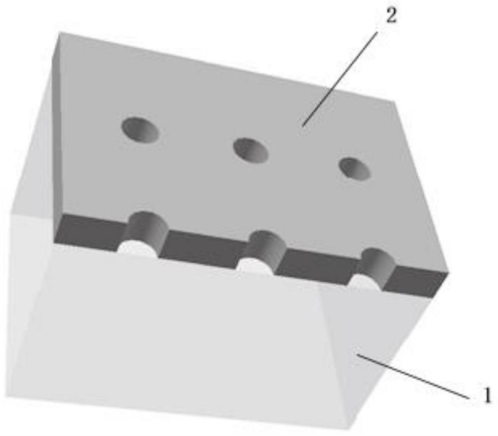
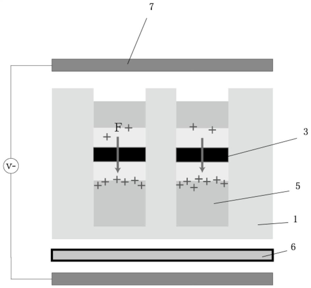
[0027] S1. A photoresist template 2 is set on the silicon base 1 as a mask for the silicon base 1, and a catalyst layer 3 is placed on the photoresist template 2. The catalyst layer is composed of a noble metal catalyst layer 3-1 and a magnetic layer 3-2. , the noble metal catalyst layer 3-1 is located on the upper and lower sides of the magnetic layer 3-2.

[0028] S2. Place the electromagnet 6 under the silicon base 1, the electromagnet 6 and the magnetic layer 3-2 are located on opposite sides of the silicon base 1;

[0029] S3. Add electrode plates 7 on the upper and lower sides of the silicon base 1, and connect a DC power supply.

[0030] The noble metal catalyst layer 3-1 is Au, the mag...


PUM


Abstract

The invention relates to an electromagnetic field coupling high aspect ratio silicon substrate etching method which comprises the following steps that S1, a photoresist template is arranged on a silicon substrate to serve as a mask of the silicon substrate, a catalyst layer is placed on the photoresist template, the catalyst layer is composed of noble metal catalyst layers and a magnetic layer, and the noble metal catalyst layers are located on the upper side and the lower side of the magnetic layer; S2, an electromagnet is placed below the silicon substrate, and the electromagnet and the magnetic layer are arranged on the two opposite sides of the silicon substrate; and S3, electrode plates are additionally arranged on the upper side and the lower side of the silicon substrate, and a direct-current power source is connected; compared with the prior art, the method has the following advantages: metal particles are more tightly contacted with the silicon substrate, the effective contact area of the catalyst and the silicon substrate is increased, holes generated in the silicon substrate can be dissolved as soon as possible, lattice defects are avoided, and the porosity is reduced, so that the surface quality of the cylindrical hole wall of the silicon substrate is improved; and excessive mechanical stress is prevented from being generated in the subsequent forming process.

Description

technical field [0001] The invention belongs to the technical field of micro-nano manufacturing, in particular to an electromagnetic field coupling high aspect ratio etching silicon base method. Background technique [0002] Magnetic permeable metal-assisted chemical etching is a wet etching technology for etching high aspect ratio structures on silicon substrates. This technology is essentially a redox reaction. During the use of this technology, precious metals are used Deposited on the silicon surface as a catalyst. [0003] In the wet etching technique, when the metal catalyst is deposited on the silicon base and then immersed in an aqueous hydrofluoric acid-hydrogen peroxide solution, a redox reaction occurs in which the volume of silicon under the catalyst is dissolved and the catalyst moves further into the etched cavity , to help continuous etching and form a HAR structure, the oxidation-reduction reaction on the surface of the metal catalyst generates electron hole...

Claims


Application Information

Patent Timeline
Patent Type & Authority Applications(China)
IPC IPC(8): H01L21/02
CPCH01L21/02019
Inventor 张俐楠陆凯刘红英吴立群王洪成
Owner HANGZHOU DIANZI UNIV
Why Eureka
Try Eureka