Waste treatment system for PCB

A technology for PCB circuit board and waste treatment, applied in the field of waste treatment system, can solve the problem of low copper purity

Inactive Publication Date: 2021-05-18
CHONGQING KAIGE ELECTRONICS CO LTD
View PDF3 Cites 2 Cited by
  • Summary
  • Abstract
  • Description
  • Claims
  • Application Information

AI Technical Summary

Problems solved by technology

[0005] The invention provides a waste treatment system for PCB circuit boards, which solves the technical problem of low purity of copper separated from PCB circuit board wastes in the prior art

Method used


Image

  • Waste treatment system for PCB

Examples


Embodiment 1

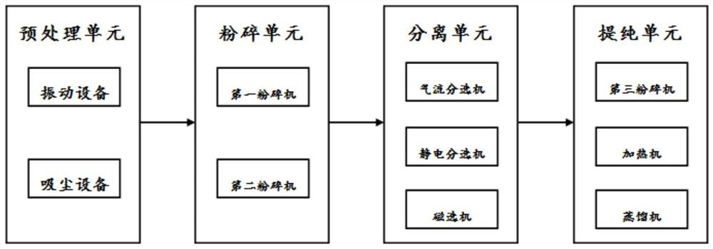
[0027] The embodiment of the waste treatment system for PCB circuit boards of the present invention is basically as attached figure 1 shown, including:

[0028] Pretreatment unit, the pretreatment unit includes vibration equipment and dust collection equipment; vibration equipment, used to vibrate the PCB circuit board; dust suction equipment, used to absorb dust generated in the vibration equipment;

[0029] The pulverizing unit includes a first pulverizer and a second pulverizer; the first pulverizer is used to pulverize the PCB circuit board into waste pieces in a first size range; the second pulverizer is used to pulverize the waste pieces into waste particles in a second size range;

[0030] Separation unit, the separation unit includes airflow separator, electrostatic separator and magnetic separator; airflow separator is used to divide waste particles into metal particles with high density and non-metallic particles with low density according to the characteristics of ...

Embodiment 2

[0046] The only difference from Example 1 is that

[0047] The purification unit also includes a first motor, a second motor and a condenser, and the first motor and the second motor are respectively connected to a heating machine and a distillation machine. During the process of heating the metal powder by the heating machine at a temperature of 250 ° C, the first motor drives the heating machine to rotate, and the molten solder will sink to the bottom of the heating machine with the help of centrifugal force, which is conducive to the separation of solder; in the distillation machine In the process of distilling the metal powder after the separation of solder at a temperature of 1000 ° C, the second motor drives the distillation machine to rotate, and the zinc and copper are dispersed with the help of centrifugal force to increase the heating area of ​​zinc, thereby speeding up the distillation speed. The condenser is located above the distillation machine, and converts the ...

Embodiment 3

[0050] The only difference from Embodiment 2 is that before the PCB circuit board is shredded, it is first judged whether the shredding can be started. That is, blow and dust the PCB circuit board first, then detect the concentration of dust near the surface of the PCB circuit board, and judge whether it is lower than the concentration threshold: if the concentration of dust near the surface of the PCB circuit board is lower than the concentration threshold, the crushing can be started; If the concentration of dust near the surface of the PCB is not lower than the concentration threshold, crushing cannot be started.

[0051] In this embodiment, after the PCB circuit board is blown and dust removed, parallel monochromatic light is used to irradiate the vicinity of the PCB circuit board surface, and the relative attenuation rate of the incident light near the PCB circuit board surface is detected. Since the dust will produce light scattering phenomenon under the irradiation of l...


PUM

PropertyMeasurementUnit
sizeaaaaaaaaaa

Abstract

The invention relates to the technical field of circuit board recovery treatment, in particular to a waste treatment system for a PCB. The system comprises a first crusher for crushing the PCB into waste fragments, a second crusher used for crushing the waste fragments into waste particles, an airflow sorting machine used for dividing the waste particles into metal particles with high density and non-metal particles with low density, an electrostatic separator used for separating the metal particles from the non-metal particles, a magnetic separator used for removing iron from the metal particles, a third crusher used for crushing the metal particles subjected to iron removal into metal powder, a heating machine and a distillation machine. The heating machine is used for heating the metal powder, so that soldering tin is melted, copper and zinc are not melted, and the soldering tin is separated; and the distillation machine is used for distilling the metal powder after the soldering tin is separated, so that zinc is evaporated and gasified, and pure copper is obtained. The technical problem that in the prior art, the purity of copper separated from the PCB waste is not high is solved through the system.

Description

technical field [0001] The invention relates to the technical field of circuit board recycling and processing, in particular to a waste processing system for PCB circuit boards. Background technique [0002] The development of science and technology has shortened the replacement cycle of electronic products, so that a large number of electronic products become electronic waste after they are scrapped. These electronic waste usually contain rare and precious metals (such as nickel) and other basic metals (such as copper, iron), and still have Very high economic value. For electronic products, PCB circuit boards are the basic components. Relevant statistics show that 1 ton of waste circuit boards contains about 130kg copper, 66kg aluminum, 0.45kg gold, 41kg iron, 30kg lead, 20kg tin, 18kg nickel, etc. It can be seen that the waste of circuit boards can be recycled to a high degree, and it is necessary to recycle them. [0003] In this regard, the document CN110496691A disclo...

Claims


Application Information

Patent Timeline
Patent Type & Authority Applications(China)
IPC IPC(8): C22B7/00C22B25/02C22B25/06C22B19/16C22B15/00B02C19/00B02C23/14
CPCC22B7/004C22B25/02C22B25/06C22B19/16C22B15/0056B02C19/00B02C23/14Y02P10/20
Inventor 李帮强
Owner CHONGQING KAIGE ELECTRONICS CO LTD
Why Eureka
Try Eureka