Gallium nitride PN diode with high blocking voltage and preparation method thereof

A gallium nitride and diode technology, applied in the direction of diodes, circuits, electrical components, etc., can solve the problems of insufficient preparation of large-scale self-supporting gallium nitride epitaxial wafers, limiting the performance and application of gallium nitride PN diodes, etc.

Active Publication Date: 2021-05-18
YANGZHOU YANGJIE ELECTRONIC TECH CO LTD
View PDF7 Cites 0 Cited by
  • Summary
  • Abstract
  • Description
  • Claims
  • Application Information

AI Technical Summary

Problems solved by technology

[0005] Vertical-structure GaN PN diodes are fabricated on homoepitaxial GaN semiconductor substrates. Vertical-structure GaN PN diodes in the current technology generally increase the length of the drift region by increasing the thickness of the epitaxial layer to obtain higher The blocking voltage, but the defec...

Method used


Image

  • Gallium nitride PN diode with high blocking voltage and preparation method thereof
  • Gallium nitride PN diode with high blocking voltage and preparation method thereof
  • Gallium nitride PN diode with high blocking voltage and preparation method thereof

Examples


Embodiment Construction

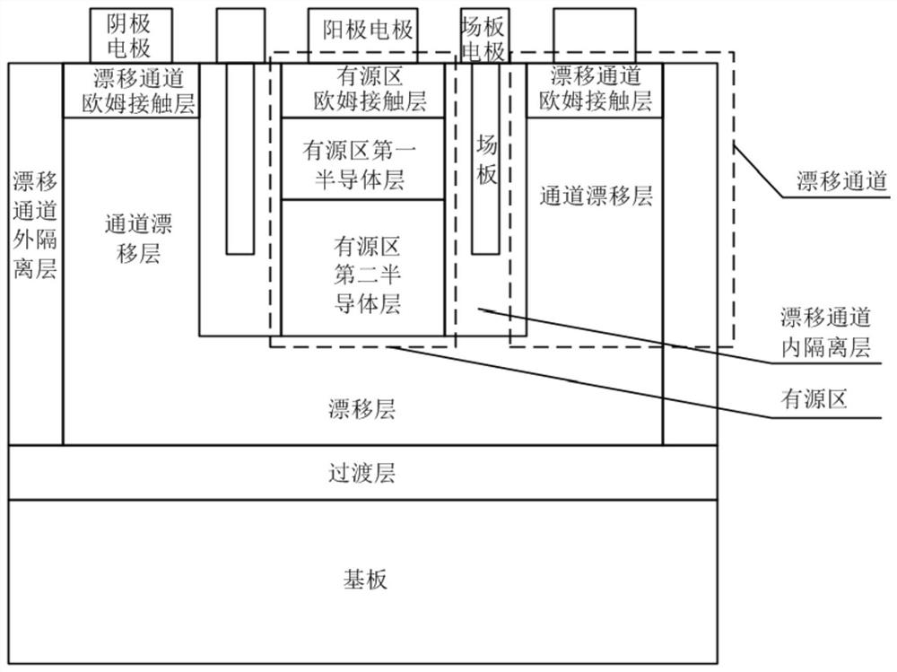
[0052]Embodiments of the present invention are described in detail below, examples of which are shown in the drawings, wherein the same or similar reference numerals designate the same or similar elements or elements having the same or similar functions throughout. The embodiments described below by referring to the figures are exemplary only for explaining the present invention and should not be construed as limiting the present invention.

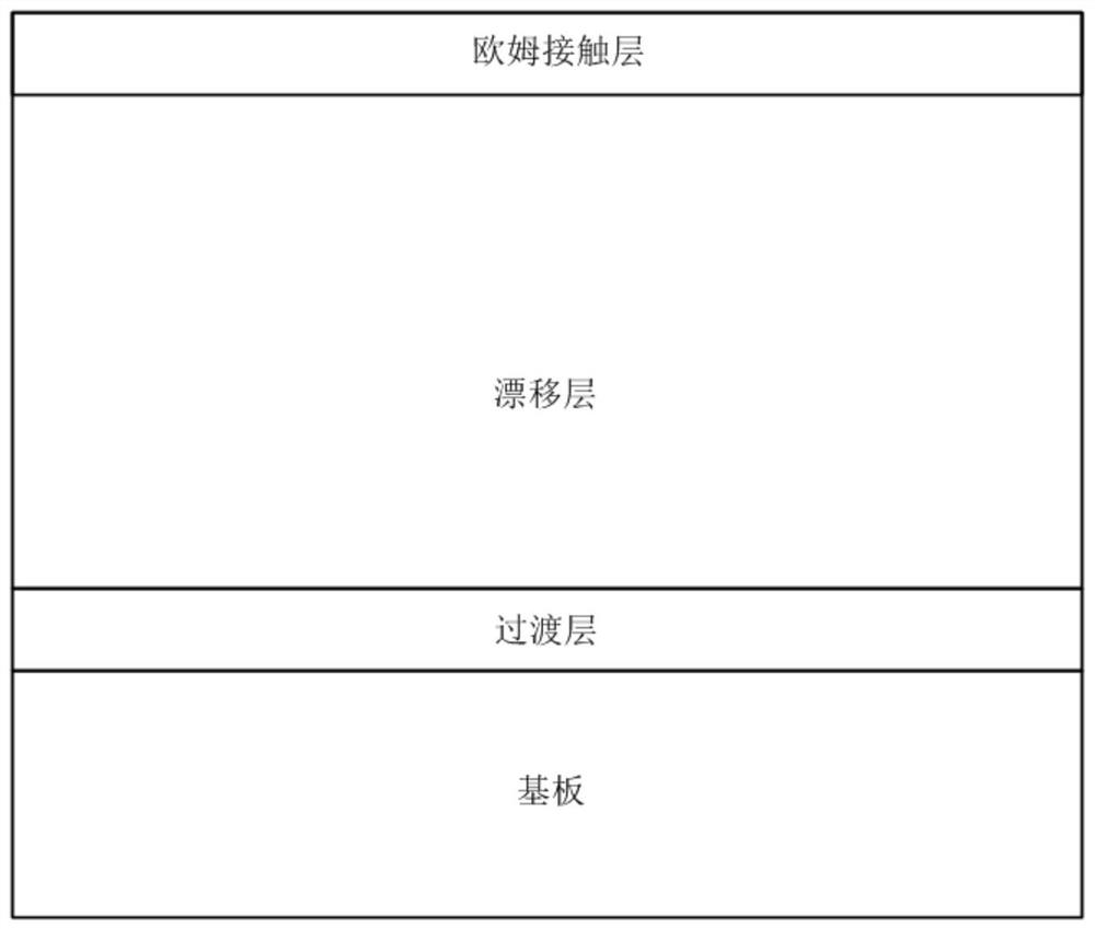
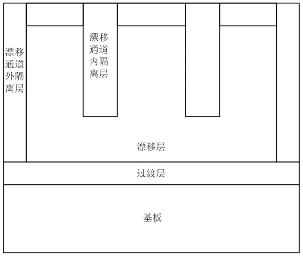
[0053] The present invention as Figure 1-6 Shown, a kind of gallium nitride PN diode preparation method of high blocking voltage comprises the following steps:

[0054] 1) Prepare a 6-inch Si substrate, SiC substrate or sapphire substrate;

[0055] 2) growing a 0.5 μm thick AlN transition layer on the substrate by metal organic chemical vapor deposition (MOCVD);

[0056] 3) Grow 8 μm thick N on the transition layer by MOCVD method ― -GaN drift layer with Si doping concentration of 1 x10 16 cm -3 (including channel drift layer);

...


PUM


Abstract

The invention discloses a gallium nitride PN diode with high blocking voltage and a preparation method, and relates to a gallium nitride power semiconductor device. The diode comprises a substrate, a transition layer, a drift layer, an active region, a drift channel, a field plate and a metal electrode layer, an annular drift region structure is formed by the second semiconductor layer in the active region, the drift layer and the two drift channels, and compared with a transverse structure gallium nitride PN diode only provided with a transverse drift region or a vertical structure gallium nitride PN diode only provided with a vertical drift region, the total path length of the drift region is greater than the path length of the drift region in a gallium nitride PN diode with a transverse structure or a vertical structure which is manufactured on the same substrate and epitaxial layer size, so that the blocking voltage of the gallium nitride PN diode is increased. The diode has the characteristics that the blocking voltage of the device is improved, the anode electrode, the cathode electrode and the field plate electrode are gathered on the top surface of the device structure to form a coplanar device input/output electrode structure, and the planar integration of the device and the application of the device in a power integrated circuit can be conveniently realized.

Description

technical field [0001] The invention relates to a gallium nitride power semiconductor device, in particular to a gallium nitride PN diode with high blocking voltage and a preparation method thereof, belonging to the technical field of power electronic devices. Background technique [0002] As a typical representative of the third-generation semiconductor, gallium nitride semiconductor has the advantages of large band gap, high breakdown electric field, high thermal conductivity, high electron saturation drift rate, and strong radiation resistance. Gallium nitride PN diodes have the advantages of high resistance Excellent characteristics such as cut-off voltage, low reverse leakage current, and high switching speed have a wide range of applications in power management, 5G mobile communications, semiconductor lighting, consumer electronics and other fields. [0003] Gallium nitride PN diodes in the current technology mainly adopt two structural forms: horizontal and vertical. ...

Claims


Application Information

Patent Timeline
IPC IPC(8): H01L21/329H01L29/06H01L29/861
CPCH01L29/0615H01L29/0684H01L29/8613H01L29/66204Y02P70/50
Inventor 赵成韩亚孙越王思元王毅
Owner YANGZHOU YANGJIE ELECTRONIC TECH CO LTD
Why Eureka
Try Eureka