Method for preparing high-crystallinity AlN thin film by growing seed crystal layer through ALD (Atomic Layer Deposition)

A seed layer and thin film technology, which is applied in the field of high crystallization AlN thin film preparation, can solve the problems of long preparation time, slow film growth rate and high cost, and achieve the effect of reducing deposition time and efficient preparation

Pending Publication Date: 2021-05-28
FUDAN UNIV
View PDF5 Cites 0 Cited by
  • Summary
  • Abstract
  • Description
  • Claims
  • Application Information

AI Technical Summary

Problems solved by technology

However, the disadvantage of ALD is that the growth rate of the film is very slow. If it is necessary to prepare an AlN film with a certain thickness for FBAR, it will take a long preparation time and the cost is relatively high.

Method used


Image

  • Method for preparing high-crystallinity AlN thin film by growing seed crystal layer through ALD (Atomic Layer Deposition)
  • Method for preparing high-crystallinity AlN thin film by growing seed crystal layer through ALD (Atomic Layer Deposition)

Examples


Embodiment 1

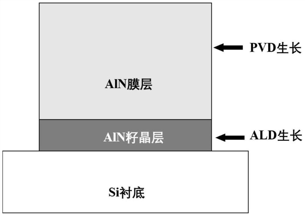
[0039] In this embodiment, an ALD combined with PVD method is used to deposit an AlN thin film. During ALD deposition of the seed layer, trimethylaluminum (TMA) and NH 3 Alternative deposition of TMA and NH as reactive precursors for Al and N sources 3 The plasma is used to grow the AlN atomic layer. During the deposition process, each ALD cycle consists of four steps: (1) TMA pulse, (2) argon purge, (3) NH 3 Pulse, (4) Argon purge. Four steps are performed to deposit a thin film of one atomic layer.

[0040] Through the above description, the specific implementation steps of the invention are as follows:

[0041] Step 1: Substrate Cleaning

[0042] Prepare single crystal Si substrate: 4-inch substrate, polished on one side, cleaned by RCA standard process, then soaked in 5% hydrofluoric acid aqueous solution for 2 minutes to remove the surface oxide layer, finally blown dry with nitrogen, and put it into the ALD chamber.

[0043] Step 2: Growth of AlN seed layer by ALD ...

Embodiment 2

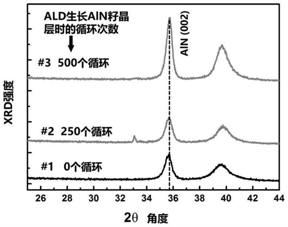
[0062] In step f in Example 1, steps b, c, d, and e are executed in cycles of 0, 250 and 500 times respectively to obtain AlN seed layers with different thicknesses, and then use PVD on the AlN seed layer with the same deposition process parameters A 1000nm AlN film layer is deposited to obtain AlN films with different crystallization degrees. as follows figure 2 As shown, the experiment proves that the c-axis orientation (002) crystal orientation of the finally prepared AlN thin film is enhanced with the increase of the number of cycles of ALD in growing the AlN seed layer.


PUM

PropertyMeasurementUnit
breakdown field strengthaaaaaaaaaa

Abstract

The invention relates to the field of AlN films, in particular to a method for preparing a high-crystallization AlN thin film by growing a seed crystal layer through ALD. Specifically, the method for preparing the AlN thin film growing on a substrate sequentially comprises the following steps: cleaning the substrate; growing the AlN seed crystal layer by using an ALD deposition method; and growing an AlN film layer on the AlN seed crystal layer by using a PVD (Physical Vapor Deposition) method to obtain the AlN thin film. According to the method, the ALD mode and the PVD mode are combined, thus, the high-crystallinity AlN thin film is prepared, specifically, the seed crystal layer grows firstly, then the thick AlN film layer is further rapidly deposited on the seed crystal layer in the PVD mode, the deposition time is further shortened, and the high-crystallinity AlN thin film can be efficiently prepared through the technology disclosed by the invention.

Description

technical field [0001] The invention relates to the field of AlN thin films, in particular to a method for preparing a highly crystalline AlN thin film using ALD to grow a seed layer. [0002] technical background [0003] Currently, the rapid development of personal communication systems, satellite transmissions, and other types of unlimited data communications has increased the center frequency of communication equipment to the GHz level. In the GHz frequency band, higher performance and integrated miniature filters are required to adapt to it. The traditional solution is to use microwave dielectric ceramic filter and surface acoustic filter (SAW). However, ceramic filters and SAW filters have some defects. For example, although ceramic filters have good performance, they are too large due to the limitation of micro-fabrication technology; Disadvantages such as low capacity. In order to overcome the above problems, the film bulk acoustic resonator (FBAR) came into being....

Claims


Application Information

Patent Timeline
Patent Type & Authority Applications(China)
IPC IPC(8): C23C16/455C23C14/35C23C14/06C23C16/34
CPCC23C14/0641C23C14/35C23C16/34C23C16/45525
Inventor 马宏平
Owner FUDAN UNIV
Why Eureka
Try Eureka