
Eureka
For R&D, Eureka makes reading and utilizing patents & technical documents easy.
Eureka AIR
Designed for self-driven R&D workflows. Generate viable solutions, solve complex R&D challenges, empower your innovation with AI.

Eureka Materials
Designed for material experts only. Revolutionize your material R&D, from search, analyze, to developing new materials.

TechResearch
Generate reliable direction feasibility study reports for your R&D in just a few steps.

TechSeek
Discover and master advanced knowledge NOW. Basics, ideas, possibilities, all at once.

TechMind
As an expert in R&D Theories, TechMind can generates customized viable solutions instantly.

TechRisk
Analyze your overall solution with one click, know your potential R&D risks in advance.

TechMonitor
Get weekly tech updates, stay abreast of the latest tech innovations and key insights.
Preparation method of epitaxial growth lanthanum nickelate and lanthanum strontium manganese oxide film
A thin-film and epitaxy technology, used in oxide conductors, non-metallic conductors, liquid chemical plating, etc., can solve problems such as difficult to control metal salt hydrolysis, harsh conditions, and complex processes
- Summary
- Abstract
- Description
- Claims
- Application Information
AI Technical Summary
Problems solved by technology
Method used
Image

Examples
Embodiment 1
[0056] NeO 3 / SrTiO 3 (100) Film preparation
[0057] Specifically include the following steps:
[0058] (1) Weigh 0.584g of polyethyleneimine and 0.584g of ethylenediaminetetraacetic acid and dissolve them in 20mL of deionized water, and stir evenly;
[0059] (2) Add 0.316g of lanthanum acetate and 0.249g of nickel acetate and stir to dissolve in the above solution, and continue to stir for 10h at room temperature to obtain a precursor solution;
[0060] (3) Spin the precursor solution on SrTiO at a spin-coating speed of 5000r / min 3 (100) Spin the glue on the single crystal substrate for 30s to form a wet film;
[0061] (4) After the spin coating is completed, place the sample in the corundum ark, heat it slowly at a rate of 1°C / min in an air atmosphere, raise the temperature to 510°C, keep it for 2 hours, and then heat it up to 700°C at a rate of 5°C / min for rapid sintering 2h, cooled with the furnace, and finally produced LaNiO 3 / SrTiO 3 (100) film.
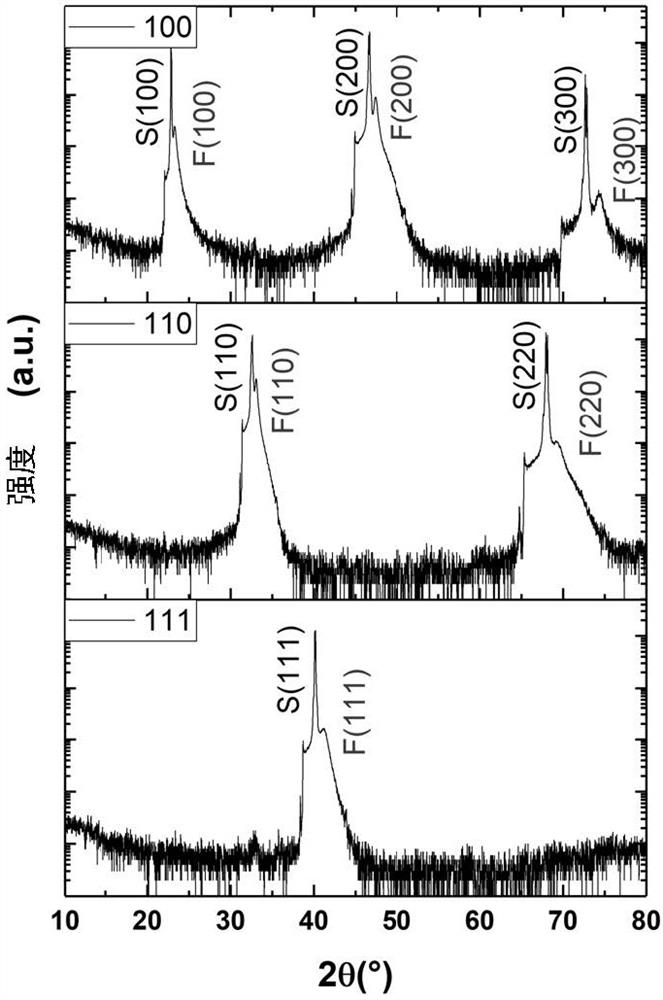
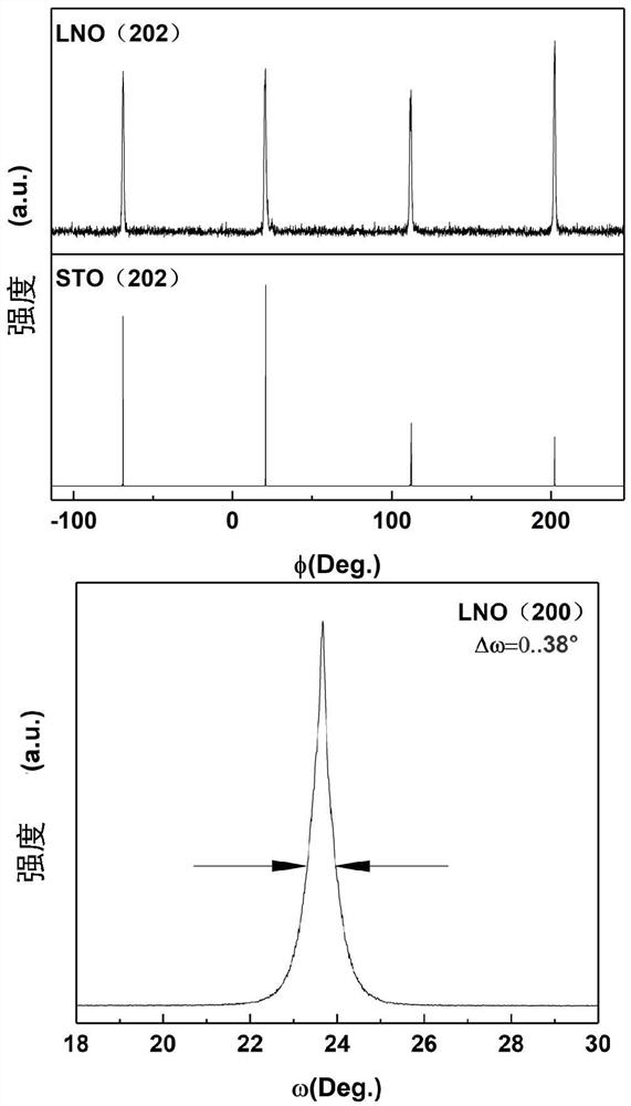
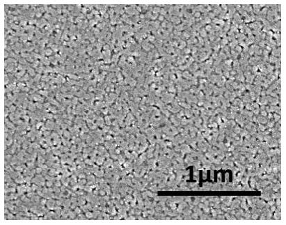
[0062] The ob...
Embodiment 2
[0070] Compared with Example 1, the difference is that in step (3), the single crystal substrate is (110) oriented SrTiO 3 , the structure of its XRD detection is as figure 1 , it can be seen that it grows with the substrate orientation. The resistivity change curve with temperature is as follows: Figure 4 .
Embodiment 3
[0072] Compared with Example 1, the difference is that in step (3), the single crystal substrate is (111) oriented SrTiO 3 , the structure of its XRD detection is as figure 1 , it can be seen that it grows with the substrate orientation. The resistivity change curve with temperature is as follows: Figure 4 .
PUM
| Property | Measurement | Unit |
|---|---|---|
| electrical resistivity | aaaaa | aaaaa |
| thickness | aaaaa | aaaaa |
| electrical resistivity | aaaaa | aaaaa |
Abstract
Description
Claims
Application Information
 - R&D Engineer
- R&D Manager
- IP Professional
- Industry Leading Data Capabilities
- Powerful AI technology
- Patent DNA Extraction
Browse by: Latest US Patents, China's latest patents, Technical Efficacy Thesaurus, Application Domain, Technology Topic, Popular Technical Reports.
© 2024 PatSnap. All rights reserved.Legal|Privacy policy|Modern Slavery Act Transparency Statement|Sitemap|About US| Contact US: help@patsnap.com