Scanning electron microscope direct-writing photoetching system based on flexible nano servo motion system

A technology of servo motion and scanning electron microscope, which is applied in the field of scanning electron microscope direct writing lithography system, can solve the problems of splicing error, high preparation cost, and difficulty in large-area preparation, so as to achieve no splicing error, avoid splicing error, and facilitate real-time observation Effect

Active Publication Date: 2021-06-01
TSINGHUA UNIV
View PDF7 Cites 1 Cited by
  • Summary
  • Abstract
  • Description
  • Claims
  • Application Information

AI Technical Summary

Problems solved by technology

[0004] The above-mentioned electron beam lithography machine has the following defects: 1) photolithography mask is required, and the preparation cost is high; 2) in-situ measurement cannot be performed; 3) the writing field is small, and it is difficult to realize large-area preparation; 4) preparation of different writing fields stitching errors

Method used


Image

  • Scanning electron microscope direct-writing photoetching system based on flexible nano servo motion system
  • Scanning electron microscope direct-writing photoetching system based on flexible nano servo motion system
  • Scanning electron microscope direct-writing photoetching system based on flexible nano servo motion system

Examples


Embodiment 1

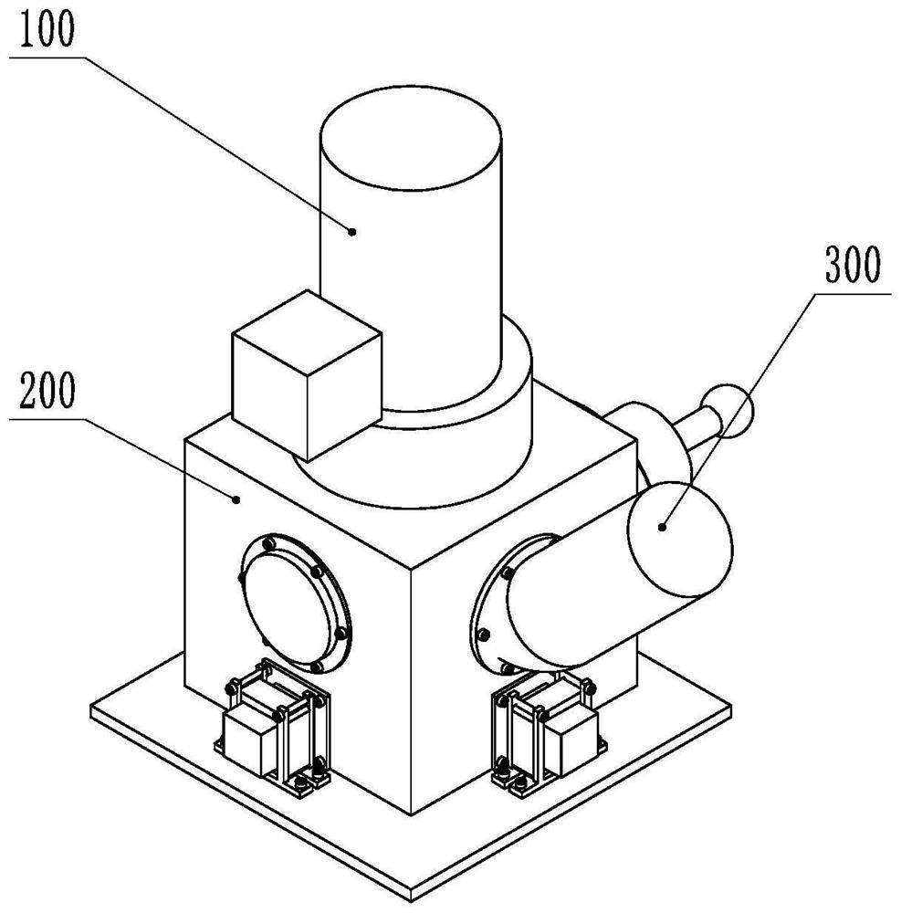
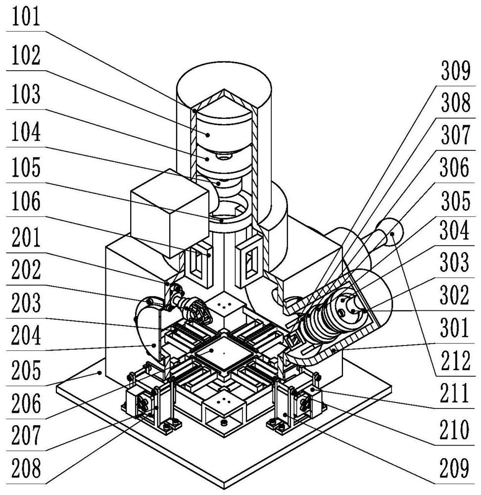
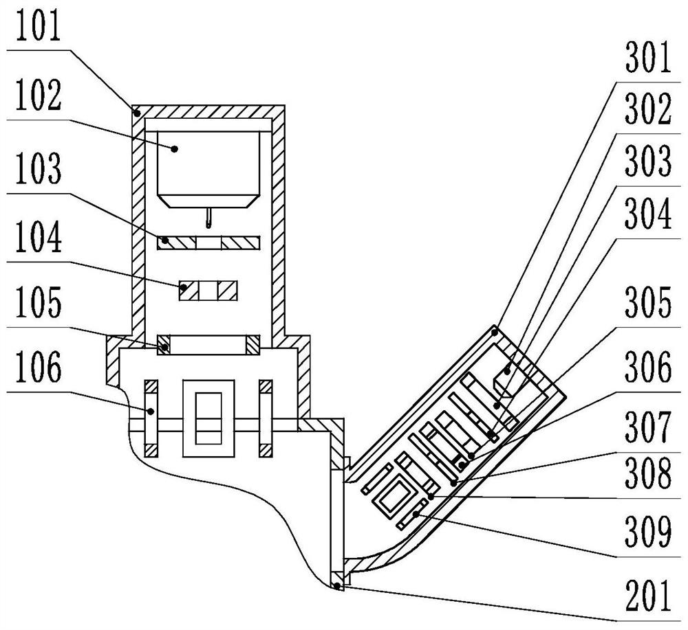
[0032] Such as Figure 1-4 As shown, a scanning electron microscope direct writing lithography system based on a flexible nano servo motion system provided in this embodiment includes an electronic chamber 100, an ion chamber 300, a sample chamber 200 and a control system.

[0033] Electron chamber 100 comprises electron chamber cavity 101, electron gun 102, anode 103, electron beam interrupter 104, electromagnetic lens 105 and electron beam deflection coil 106; Electron chamber 100 is fixedly connected with sample chamber 200; Ion chamber 300 comprises ion chamber cavity Body 301, ion source 302, suppression electrode 303, extraction electrode 304, first stage lens 305, ion beam shutter editor 306, ion beam shutter barrier film hole 307, second stage lens 308 and ion beam scanning deflection electrode 309; The chamber 300 is fixedly connected to the sample chamber 200; the sample chamber 200 includes a sample chamber cavity 201, a secondary electronic detector 202, a nano-pre...

Embodiment 2

[0047] This embodiment is basically the same as Embodiment 1. For the sake of brevity, in the description process of this embodiment, the same technical features as Embodiment 1 will not be described, and only the differences between this embodiment and Embodiment 1 will be described:

[0048] Further, a laser interferometer is also included, which is used to feed back the actual displacement of the flexible motion platform with nanometer precision, so as to realize closed-loop feedback control.

[0049] Further, it also includes a viewing window, which is arranged on the cavity of the sample chamber for observing the internal state of the cavity of the sample chamber.

[0050] In this embodiment, the scanning electron microscope direct writing lithography system based on the flexible nano-servo motion system provided in this embodiment can be prepared using ion beams and at the same time detect the preparation results through electron beams in real time. The specific preparati...


PUM


Abstract

The invention discloses a scanning electron microscope direct-writing photoetching system based on a flexible nano servo motion system. The scanning electron microscope direct-writing photoetching system comprises an electron chamber, an ion chamber, a sample chamber and a control system; the electron chamber comprises an electron chamber cavity, an electron gun, an anode, an electron beam blocker, an electromagnetic lens and an electron beam deflection coil; the ion chamber comprises an ion chamber cavity, an ion source, an ion beam scanning deflection electrode and the like; the sample chamber comprises a sample chamber cavity, a secondary electron detector, a nano-precision flexible servo motion platform system and the like; the control system comprises a computer, an electron beam scanning controller, an ion beam scanning controller and the like. The electron beam generated by the electron chamber or the ion beam generated by the ion chamber can be used for nano direct-writing preparation, and the nano-precision flexible motion platform in the sample chamber and the electron beam / ion beam can cooperatively move or be linked, so that splicing errors in preparation are avoided, and large-area nano direct-writing photoetching without splicing errors is realized. The system can also perform in-situ detection in the preparation process, so that the preparation result is convenient to observe in real time.

Description

technical field [0001] The invention relates to the field of direct writing preparation of semiconductor integrated circuits, in particular to a scanning electron microscope direct writing photolithography system based on a flexible nanometer servo motion system. Background technique [0002] At present, photolithography is the main way to achieve nanofabrication. The characteristic scale of lithography is mainly limited by the wavelength of the light source, and it is relatively difficult to achieve ten-nanometer-scale fabrication through lithography. General electron beam and ion beam lithography has the following characteristics: the preparation line width can reach several nanometers; it has a very limited writing field (about 100 microns); if it is necessary to prepare large-area nanoscale patterns, it needs to be manually or through steps. The input motor drives the sample to move, and the preparation is performed one by one; there is a large splicing error between di...

Claims


Application Information

Patent Timeline
Patent Type & Authority Applications(China)
IPC IPC(8): G03F7/20
CPCG03F7/2059G03F7/2065G03F7/704G03F7/70725G03F7/70758G03F7/70016G03F7/70033H01J37/3174H01J2237/31737H01J2237/31749H01J2237/2817
Inventor 张震刘义杰曲钧天
Owner TSINGHUA UNIV
Why Eureka
Try Eureka