Preparation method of P electrode of light-emitting diode chip with vertical structure

A light-emitting diode, vertical structure technology, applied in circuits, electrical components, semiconductor devices, etc., can solve the problems of p-GaN electrode electrode reflectivity drop, affecting electrode optical performance and other problems

Active Publication Date: 2021-06-01
HC SEMITEK ZHEJIANG CO LTD
View PDF7 Cites 3 Cited by
  • Summary
  • Abstract
  • Description
  • Claims
  • Application Information

AI Technical Summary

Problems solved by technology

[0004] In the process of realizing the present disclosure, the inventors found that the related technology has at least the following problems: the high temperature in the annealing process will lead to the agg...

Method used


Image

  • Preparation method of P electrode of light-emitting diode chip with vertical structure
  • Preparation method of P electrode of light-emitting diode chip with vertical structure
  • Preparation method of P electrode of light-emitting diode chip with vertical structure

Examples


Embodiment Construction

[0030] In order to make the objectives, technical solutions and advantages of the present disclosure clearer, the embodiments of the present disclosure will be further described in detail below with reference to the accompanying drawings.

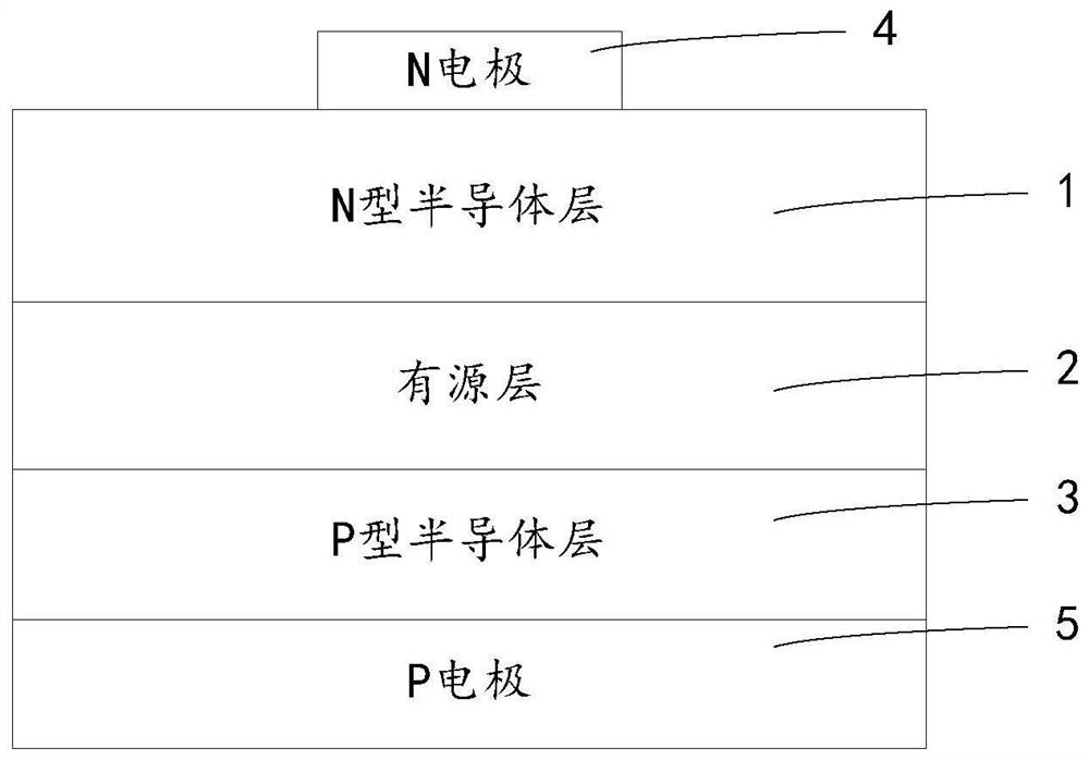
[0031] In order to facilitate the understanding of the technical solutions provided by the embodiments of the present disclosure, the structure of the vertical structure light emitting diode chip is first introduced. figure 1 It is a schematic structural diagram of a vertical structure light emitting diode chip provided by an embodiment of the present disclosure. see figure 1 , the vertical structure light-emitting diode chip includes an N-type semiconductor layer 1, an active layer 2, a P-type semiconductor layer 3, an N electrode 4 and a P electrode 5, and the N electrode 4 and the P electrode 5 are oppositely arranged. The surface where the N electrode is located is the light-emitting surface. The surface where the P electrode is locat...


PUM

PropertyMeasurementUnit
Thicknessaaaaaaaaaa
Thicknessaaaaaaaaaa
Thicknessaaaaaaaaaa

Abstract

The invention provides a preparation method of a P electrode of a light-emitting diode chip with a vertical structure, and belongs to the field of light-emitting diodes. The method comprises the steps of providing a light-emitting diode epitaxial wafer, wherein the light-emitting diode epitaxial wafer comprises a substrate, and a buffer layer, an undoped GaN layer, an N-type GaN layer, a multi-quantum well layer, an electron barrier layer, a P-type GaN layer and a P-type ohmic contact layer which are stacked on the substrate in sequence, wherein a contact layer electrode is grown on the P-type ohmic contact layer, thermal annealing treatment is conducted on the contact layer electrode, and the contact layer electrode comprises a Ni layer; and a first reflecting layer electrode is grown on the contact layer electrode, thermal annealing treatment is conducted on the first reflecting layer electrode, the first reflecting layer electrode comprises a first Ag layer, the annealing time of the first reflecting layer electrode is shorter than that of the contact layer electrode, and the annealing temperature of the first reflecting layer electrode is lower than that of the contact layer electrode. According to the invention, the P electrode with high reflectivity and low contact resistivity can be obtained.

Description

technical field [0001] The present disclosure relates to the field of light emitting diodes, and in particular, to a method for preparing a P electrode of a vertical structure light emitting diode chip. Background technique [0002] The two electrodes of the vertical structure LED (Light Emitting Diode, light emitting diode) chip are respectively on two sides of the LED epitaxial layer. At present, a key difficulty of vertical structure LEDs is the p-type ohmic contact. Taking GaN-based vertical structure LEDs as an example, on the one hand, due to the high activation energy of Mg, it is difficult to obtain p-GaN with high hole concentration, on the other hand, The p-GaN electrode of a GaN-based LED with a vertical structure serves as both an ohmic contact electrode and an optical mirror, which puts forward very high requirements on the material system of the electrode. Therefore, p-GaN electrodes with good ohmic contact and high reflectivity are crucial for GaN-based LEDs ...

Claims


Application Information

Patent Timeline
IPC IPC(8): H01L33/40
CPCH01L33/40H01L33/405H01L2933/0016
Inventor 刘旺平梅劲刘春杨张武斌葛永晖
Owner HC SEMITEK ZHEJIANG CO LTD
Why Eureka
Try Eureka