Mesa PiN diode and production method, and silicon-based reconfigurable stealth antenna
A diode and mesa technology, used in antennas, radiating element structures, semiconductor/solid-state device manufacturing, etc., can solve problems such as poor distribution uniformity, low carrier concentration, and large electrode ratio, and achieve large and good breakdown voltage. The effect of device performance and practicability
- Summary
- Abstract
- Description
- Claims
- Application Information
AI Technical Summary
Problems solved by technology
Method used
Image

Examples
Embodiment 1
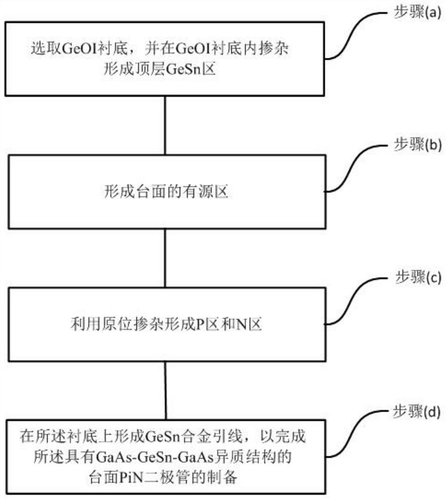
[0054] See figure 1 , figure 1 It is a flow chart of a method for preparing a mesa PiN diode according to an embodiment of the present invention. This method is suitable for preparing a mesa PiN diode with a GaAs-GeSn-GaAs heterostructure, and the diode is mainly used for making silicon-based reconfigurable stealth Antenna, the method includes the steps of:
[0055] (a) select a GeOI substrate, and dope in the GeOI substrate to form a top GeSn region;
[0056] (b) forming the active region of the mesa;
[0057] (c) forming a P region and an N region by in-situ doping;
[0058] (d) forming GeSn alloy leads on the substrate to complete the preparation of the mesa PiN diode with GaAs-GeSn-GaAs heterostructure.
[0059] Wherein, for step (a), the reason for doping the top layer GeSn region in the GeOI substrate is that, for the silicon-based solid-state plasma antenna, since it requires good microwave characteristics, its radiating unit diode needs to have a high concentration...
Embodiment 2
[0098] See Figure 2a-Figure 2t , Figure 2a-Figure 2t It is a schematic diagram of a preparation method of a mesa PiN diode according to an embodiment of the present invention. On the basis of the first embodiment above, the preparation of a mesa PiN diode with a GaAs-GeSn-GaAs heterostructure with a solid-state plasma region length of 120 microns is For example, the length of the intrinsic region can be between 50 microns and 150 microns, and the specific steps are as follows:
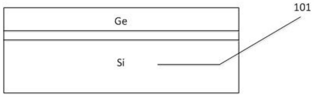
[0099] S10, selecting a GeOI substrate.
[0100] See Figure 2a , the crystal orientation of the GeOI substrate 101 is (110), in addition, the doping type of the GeOI substrate 101 is p-type, and the doping concentration is 5×10 14 cm -3 , the thickness of the top layer Ge is 50 μm.
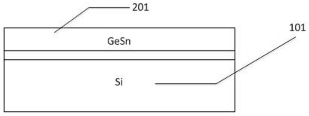
[0101] S20, doping into the GeOI substrate to form a top-layer GeSn region.
[0102] See Figure 2b , the specific method may be: photoetching the GeOI substrate, doping the GeOI substrate with Sn composition, so...
Embodiment 3
[0140] See image 3 , image 3 It is a schematic diagram of the device structure of a mesa PiN diode according to an embodiment of the present invention, and the PiN diode adopts the above-mentioned figure 1 prepared as indicated.
[0141] Specifically, the mesa PiN diode is prepared and formed on a GeOI substrate 301, and the P region 303, the N region 304 of the PiN diode and the intrinsic region laterally located between the P region 303 and the N region 304 are all located on the substrate within the top GeSn region 302 .
[0142] The invention discloses a mesa PiN diode, a preparation method and a silicon-based reconfigurable stealth antenna. A mesa structure is introduced into the PiN diode to change the structure of the active region, and specifically adjusts the ratio of the P region and the N region relative to the intrinsic region. The position reduces the proportion of the electrode in the diode, and greatly improves the influence of the solid-state plasma region...
PUM
| Property | Measurement | Unit |
|---|---|---|
| thickness | aaaaa | aaaaa |
| thickness | aaaaa | aaaaa |
Abstract
Description
Claims
Application Information
 - R&D
- Intellectual Property
- Life Sciences
- Materials
- Tech Scout
- Unparalleled Data Quality
- Higher Quality Content
- 60% Fewer Hallucinations
Browse by: Latest US Patents, China's latest patents, Technical Efficacy Thesaurus, Application Domain, Technology Topic, Popular Technical Reports.
© 2025 PatSnap. All rights reserved.Legal|Privacy policy|Modern Slavery Act Transparency Statement|Sitemap|About US| Contact US: help@patsnap.com