A method and device for preparing black silicon

A technology of black silicon and silicon materials, applied in the field of semiconductor optoelectronic materials, can solve the problems of difficult engineering application, difficult mass production, affecting the processing efficiency of black silicon, etc., and achieve the effect of good absorption rate and short pulse width

Active Publication Date: 2021-08-24
WUHAN HGLASER ENG CO LTD
View PDF0 Cites 0 Cited by
  • Summary
  • Abstract
  • Description
  • Claims
  • Application Information

AI Technical Summary

Problems solved by technology

However, most 800nm ​​lasers are research-grade lasers, which have major problems in terms of stability and integration, making it difficult to realize engineering applications. Moreover, the repetition rate of 800nm ​​femtosecond lasers is very low, generally only 1kHz, which will greatly affect The processing efficiency of black silicon is difficult to achieve mass production

Method used


Image

  • A method and device for preparing black silicon
  • A method and device for preparing black silicon
  • A method and device for preparing black silicon

Examples


Embodiment approach

[0059] As an embodiment, the method for preparing black silicon includes the following steps:

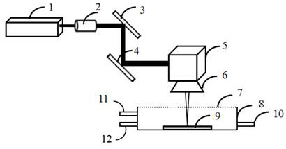
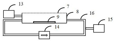
[0060] Step 1, place the silicon material 9 in a sealed gas chamber 8, use the vacuum pump 13 to extract the air in the sealed gas chamber 8 through the vacuum pumping port 11, close the vacuum pumping port 11 and the vacuum pump 13 after the pumping is completed, and then open Gas source 15 access gas.

[0061] Step 2, the laser beam emitted by the ultrafast laser 1 passes through the beam expander collimating mirror 2, the first reflector 3 and the second reflector 4, enters the high-speed galvanometer 5, and then focuses through the field mirror 6, as figure 1 As shown, wherein, the wavelength of the ultrafast laser 1 is 1030nm or 1064nm, and the pulse width is less than 12ps. The focused beam passes through the laser light opening 7 at the top of the airtight gas chamber 8 and focuses on the surface of the silicon material 9 or above the silicon material 9 , which is not lim...

Embodiment 1

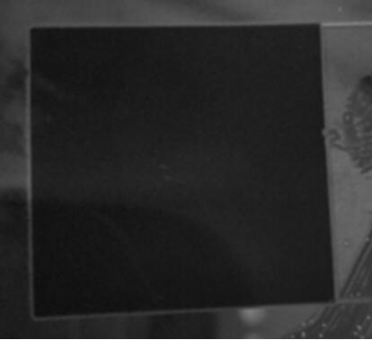
[0066] This embodiment provides a method for preparing black silicon, using an ultrafast infrared laser with a wavelength of 1030nm and a pulse width of 480fs to The silicon wafer area is etched, the laser repetition frequency is 100kHz, and the diameter of the active spot is adjusted to , the spot energy density is , the horizontal and vertical overlapping ratios of the facula are set to 93%. Processed samples such as image 3 As shown, it can be seen that the whole etched area has a high degree of blackening, which is in obvious contrast with the surrounding original materials. Observing the microscopic morphology of the etched area through a confocal microscope, it was found that the entire area is composed of a large number of pointed cone-shaped microstructures, which are clear and dense as a whole, such as Figure 4 As shown, the height measurement shows that the heights of these conical microstructures are about. Finally, the absorbance of the sample to the 400...

Embodiment 2

[0068] This embodiment provides a method for preparing black silicon, using an ultrafast infrared laser with a wavelength of 1064nm and a pulse width of 1ps to The silicon wafer area is etched, the laser repetition frequency is 175kHz, and the diameter of the active spot is adjusted to , the spot energy density is , the horizontal and vertical overlapping ratios of the facula are set to 95%. Processed samples such as Image 6 As shown, it can be seen that the whole etched area has a high degree of blackening, which is in obvious contrast with the surrounding original materials. Observing the microscopic morphology of the etched area through a confocal microscope, it was found that the entire area is composed of a large number of pointed cone-shaped microstructures, which are clear and dense as a whole, such as Figure 7 As shown, the height measurement shows that the heights of these conical microstructures are about. Finally, the absorbance of the sample to the 400nm...


PUM

PropertyMeasurementUnit
diameteraaaaaaaaaa
heightaaaaaaaaaa
wavelengthaaaaaaaaaa

Abstract

The invention discloses a method and device for preparing black silicon. A laser port is provided above a sealed gas cavity for laser injection, a vacuum pumping port is provided for vacuuming, a gas input port is provided for introducing gas, and a dust extraction port is provided. The output port is used to extract the gas containing dust. The gas input port, the dust extraction output port and the external circulation pipeline form a circulation channel, and a dust filter device is installed on the external circulation pipeline to filter the dust of the gas at the dust extraction output port; The silicon wafer is placed in a closed gas chamber. After vacuuming and feeding the gas, the cycle is started, the laser is started, and the laser is focused on or above the silicon wafer surface. The laser interacts with the silicon wafer and the gas to form a sharp cone on the silicon wafer surface. shape microstructure and S atom doping; the invention adjusts the etching efficiency of the silicon wafer by adjusting the horizontal and vertical overlapping ratio of the light spot, the diameter of the light spot and the laser repetition frequency, so as to meet the requirements of the energy density of the light spot for the melting of the silicon material and meet the requirements of the black spot. Silicon industrialization requires etching efficiency.

Description

technical field [0001] The invention relates to the technical field of semiconductor optoelectronic materials, in particular to a method and device for preparing black silicon. Background technique [0002] The special chemical properties of silicon determine that silicon is an excellent semiconductor material. It is rich in resources, and its content in the earth's crust is second only to oxygen, about 27.6%. It is also easy to purify, easy to dope, and high temperature resistant. Therefore, it is widely used in the semiconductor industry and becomes the main production material of optoelectronic devices. However, the surface of crystalline silicon has a high reflection of ultraviolet-infrared light. If the surface of crystalline silicon is not treated, it can reflect more than 30% of visible-infrared light and more than 50% of ultraviolet light. In the existing industrial production, the surface reflectance of monocrystalline silicon and polycrystalline silicon after text...

Claims


Application Information

Patent Timeline
Patent Type & Authority Patents(China)
IPC IPC(8): H01L31/18B23K26/352H01L31/0236H01L31/028
CPCB23K26/355H01L31/02363H01L31/028H01L31/1804Y02P70/50
Inventor 王雪辉陈航冯新康
Owner WUHAN HGLASER ENG CO LTD
Why Eureka
Try Eureka