A two-dimensional semiconductor material snse 2 Single crystal preparation method

A two-dimensional semiconductor and single crystal technology, applied in the field of two-dimensional materials, can solve the problems of limited development, unavailability, high quality, etc., and achieve the effect of simple and easy preparation process, simple equipment, and improved preparation efficiency

Active Publication Date: 2022-03-25
NANJING TECH UNIV
View PDF3 Cites 0 Cited by
  • Summary
  • Abstract
  • Description
  • Claims
  • Application Information

AI Technical Summary

Problems solved by technology

The preparation of SnSe reported today 2 Single crystal method, due to the presence of inappropriate precursors or mixed products after the reaction, the product has defects, so that large-area, high-quality 2D intrinsic SnSe cannot be obtained 2 Single crystal, which further limits its development in the field of optoelectronic devices

Method used


Image

  • A two-dimensional semiconductor material snse  <sub>2</sub> Single crystal preparation method
  • A two-dimensional semiconductor material snse  <sub>2</sub> Single crystal preparation method
  • A two-dimensional semiconductor material snse  <sub>2</sub> Single crystal preparation method

Examples


Embodiment 1

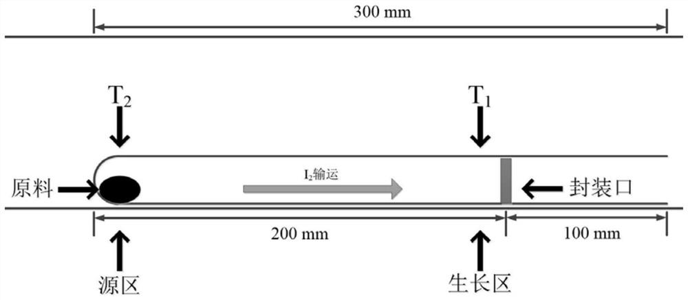
[0031] A method of chemical vapor transport (CVT) based on the preparation of sheet-like easy-to-exfoliate two-dimensional SnSe 2 Single crystal method, the steps are as follows:

[0032] Step (1), according to the molar ratio of Se powder and Sn powder is 2:1, weigh elemental selenium powder and elemental tin powder, the total mass is 1g; according to the stickiness on weighing paper, put Sn powder and Se powder into Mortar, grind in the mortar for 10-15min until the color is uniform gray-black; through the paper cylinder channel, the uniformly mixed powder sample is transported to the quartz tube (quartz tube size: length 300mm, inner diameter 25mm, seal The closed end (100mm away from the quartz nozzle) (can be called the source area);

[0033] Add an appropriate amount of iodine particles into the quartz tube as a transfer agent. Generally, the amount of iodine used in 1g of sample is 50 mg. Also, iodine particles are placed in the closed end of the quartz tube; since iod...

Embodiment 2

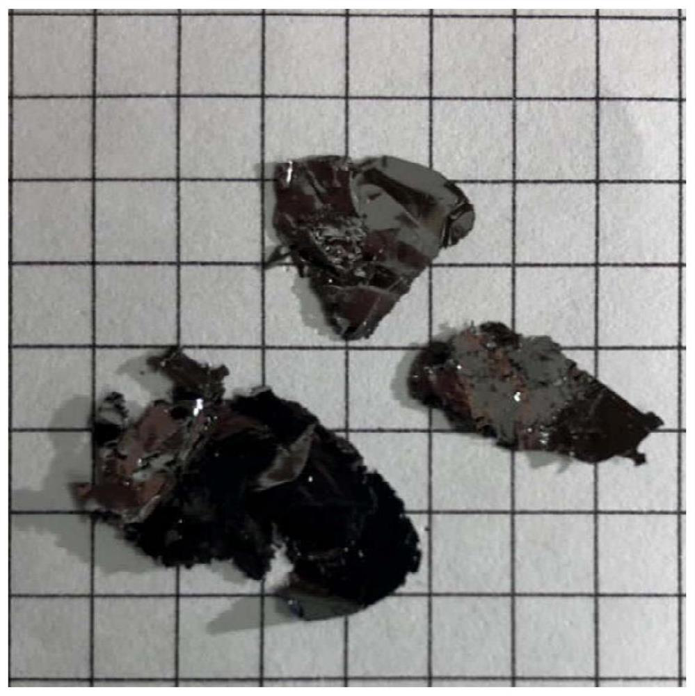
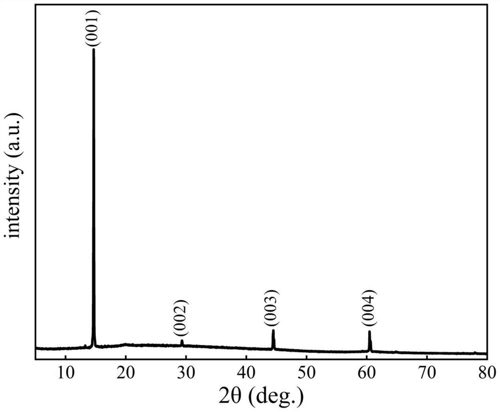
[0041] Referring to the method of Example 1, only adjust step (2) The temperature difference between the high temperature zone and the low temperature zone in the growth stage and cooling stage is maintained at 20°C, and the temperature in the low temperature zone is kept at 550°C. This embodiment can also make SnSe 2 single crystal (see Figure 5 ).

[0042] With the SnSe that embodiment 1 makes 2 Compared with single crystal, the present example SnSe 2 The area of ​​the single crystal is relatively small, and the surface is not as good as that of the SnSe prepared in Example 1. 2 Single crystal flat.


PUM


Abstract

The invention discloses a two-dimensional semiconductor material SnSe 2 Single crystal preparation method: mix Se powder and Sn powder evenly, put them into a quartz tube, put elemental iodine, pump the air pressure in the quartz tube to ≤0.1mbar, seal the tube; put the quartz tube into a double temperature zone tube furnace , put one end containing the raw material in the high temperature zone and the other end in the low temperature zone. Keep at 560-600°C for 5-7 days; then lower to room temperature, keep the temperature difference between the high-temperature zone and the low-temperature zone at 10-50°C during the cooling process, and obtain flake, large-area, high-quality SnSe 2 single crystal. The present invention can prepare SnSe in one step 2 Single crystal, single crystal is bright black, in thin sheet shape, single crystal composition is uniform, the surface is smooth, easy to mechanically peel off, which is conducive to micro-processing of materials such as photolithography.

Description

technical field [0001] The invention belongs to the field of two-dimensional materials, and relates to a two-dimensional semiconductor material SnSe 2 A method for preparing a single crystal, in particular to a method for preparing a large-area, high-quality two-dimensional intrinsic SnSe 2 single crystal method. Background technique [0002] Since Geim and Novoselov first reported the successful preparation of graphene by scotch tape peeling method in 2004, people have been working hard to find two-dimensional materials, and a huge family of two-dimensional materials has been formed. Graphene has rich and peculiar physical properties, and it has unique carrier characteristics and excellent electrical properties. The carriers in graphene are Dirac-fermions with ultrahigh carrier mobility. However, perfect graphene is a zero-bandgap semiconductor, which hinders the application of graphene in semiconductor devices. Novel two-dimensional materials—two-dimensional semiconduc...

Claims


Application Information

Patent Timeline
Patent Type & Authority Patents(China)
IPC IPC(8): C30B25/00C30B29/46C30B29/64
CPCC30B25/00C30B29/46C30B29/64
Inventor 胡小会陈旭凡
Owner NANJING TECH UNIV
Why Eureka
Try Eureka