Perovskite/crystalline silicon laminated solar cell based on double tunneling compound

A technology of solar cells and compounds, applied in the field of solar cells, can solve the problems of limiting long-term light stability, expensive manufacturing process, limiting wide application, etc., and achieve the effects of excellent photovoltaic power generation performance, improved utilization rate, and simple process flow

Pending Publication Date: 2021-06-25
HANGZHOU ZHONGNENG PHOTOELECTRIC TECH CO LTD
View PDF3 Cites 0 Cited by
  • Summary
  • Abstract
  • Description
  • Claims
  • Application Information

AI Technical Summary

Problems solved by technology

a-Si:H has a high absorption coefficient and is considered to be an excellent candidate for low-cost photovoltaics, but the unavoidable Staebler-Wronski effect limits its long-term photostability, leading to the creation of deep-site defect recombination centers
Although the power conversion efficiency of III-V multi-junction solar cells has exceeded 30%, the complex and expensive fabrication process limits their widespread application to space photovoltaics or concentrated photovoltaics

Method used


Image

  • Perovskite/crystalline silicon laminated solar cell based on double tunneling compound
  • Perovskite/crystalline silicon laminated solar cell based on double tunneling compound

Examples


Embodiment

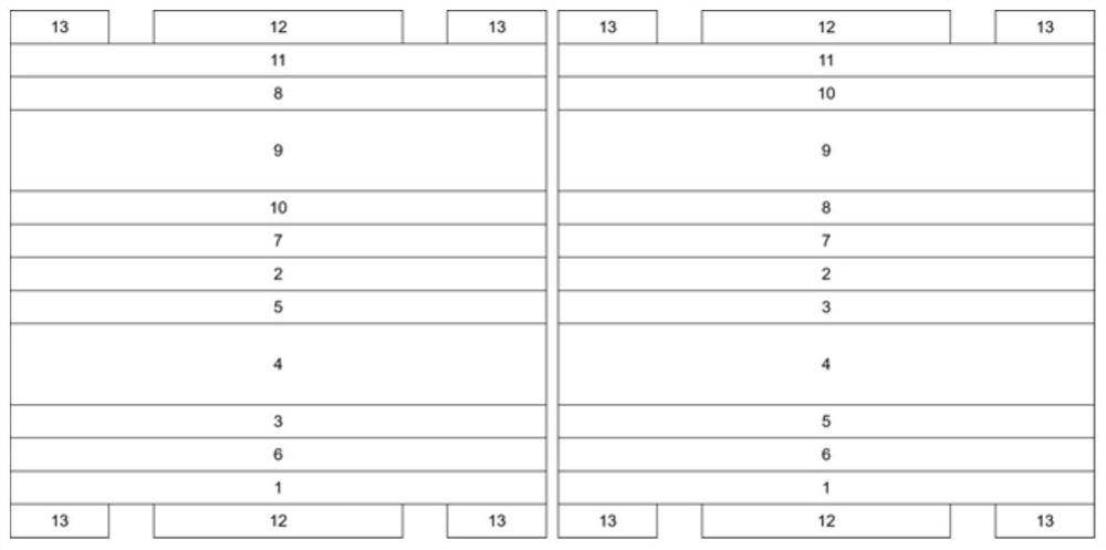
[0029] A perovskite / crystalline silicon tandem solar cell based on double tunneling compound composed of Ag grid lines, MgF 2 , ITO, p-type amorphous silicon, the first tunneling SiO 2 , P-type monocrystalline silicon wafer, second tunneling SiO 2 , n-type amorphous silicon, IZO, PTAA, (CH(NH 2 ) 2 PB 3 ) 0.83 Cs 0.17 Pb(I 0.82 Br 0.18 ) 3 (1.66 eV), C60, TiO 2 , ITO, MgF 2 and Ag grid lines, the preparation steps are as follows:

[0030] Step 1) Texturing: First, double-sided texturing is performed on a 220-micron-thick P-type monocrystalline silicon wafer, then cleaned and set aside;

[0031] Step 2) Deposit tunneling SiO on the front and back of the silicon wafer 2 Passivation contact: 1.1nm ultra-thin SiO is thermally grown on the front and back sides of a clean N-type single crystal silicon wafer 2 , cooling for later use;

[0032] Step 3) Deposit n-type amorphous silicon and p-type amorphous silicon on the front and back of the silicon wafer respectively: PEC...


PUM

PropertyMeasurementUnit
thicknessaaaaaaaaaa

Abstract

The invention discloses a perovskite / crystalline silicon laminated solar cell based on a double tunneling compound. The perovskite / crystalline silicon laminated solar cell comprises a grid line, an antireflection layer, a first transparent conductive oxide, n-type microcrystalline silicon or amorphous silicon (p-type microcrystalline silicon or amorphous silicon), a first tunneling compound, a N or P-type monocrystalline silicon wafer, a second tunneling compound, p-type microcrystalline silicon or amorphous silicon (n-type microcrystalline silicon or amorphous silicon), a second transparent conductive oxide, an electron transport layer (hole transport layer), a perovskite light absorption layer, a hole transport layer (electron transport layer), a third transparent conductive oxide, an antireflection layer and a grid line. According to the invention, tunneling compound selective contact is directly formed on the two faces of a N-type or P-type monocrystalline silicon wafer, so that the passivation effect is remarkable, the process is simple, and the cost is low; and the crystalline silicon bottom cell based on the double tunneling compound and the perovskite top cell can easily realize better current matching, interface charge transmission is smoother, and high conversion efficiency and high stability are realized at the same time.

Description

technical field [0001] The invention relates to a solar cell, in particular to a perovskite / crystalline silicon laminated solar cell based on a double tunneling compound. Background technique [0002] Global fossil resources are increasingly depleted, and solar energy is an ideal alternative due to its green and renewable nature. One of the most important utilization methods of solar energy is photovoltaic power generation technology, which directly converts solar energy into electrical energy. Improving solar cell efficiency is one of the keys to reducing the cost of photovoltaic power generation while improving its competitiveness with conventional power sources. The most direct way to improve is to fabricate multi-junction tandem solar cells composed of multiple absorbing layers with complementary band gaps. The tandem cell concept has been widely used, ranging from relatively low-cost hydrogenated amorphous silicon (a-Si:H) to the highest performance III-V component ma...

Claims


Application Information

Patent Timeline
Patent Type & Authority Applications(China)
IPC IPC(8): H01L31/0216H01L31/0256H01L31/028H01L51/42
CPCH01L31/02167H01L31/028H01L2031/0344H10K30/10Y02E10/547Y02E10/549
Inventor 徐敬超张文君石磊
Owner HANGZHOU ZHONGNENG PHOTOELECTRIC TECH CO LTD
Why Eureka
Try Eureka