A kind of aluminum quantum well laser and its preparation method

A laser and aluminum quantum technology, which is applied in the direction of lasers, phonon exciters, laser components, etc., can solve the problems of poor etching surface performance, etc., and achieve the effects of low cost, reduced oxygen content, and simple operation

Active Publication Date: 2021-08-13
SHANXI YUANJIE SEMICONDUCTOR TECH CO LTD
View PDF0 Cites 0 Cited by
  • Summary
  • Abstract
  • Description
  • Claims
  • Application Information

AI Technical Summary

Problems solved by technology

[0006] In order to solve the problem of poor stability of aluminum quantum well lasers, the present invention provides an aluminum quantum well laser and its preparation method. The preparation method of the present invention is mainly to solve the problem of poor performance caused by the oxidation of the etched surface in the process of the aluminum quantum well laser process , compared with the traditional passivation technology, the cost is low, the process is simple, and the stability is strong

Method used


Image

  • A kind of aluminum quantum well laser and its preparation method
  • A kind of aluminum quantum well laser and its preparation method
  • A kind of aluminum quantum well laser and its preparation method

Examples


preparation example Construction

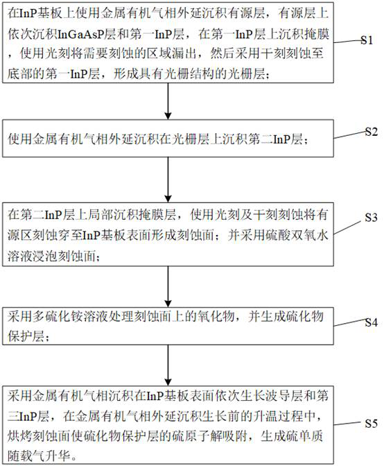
[0052] Such as figure 1 Shown, the first object of the present invention is to provide a kind of preparation method of aluminum quantum well laser, comprises the following steps:

[0053] Step 1: Deposit the active layer on the InP substrate using metal-organic vapor phase epitaxy, deposit an InGaAsP layer and a first InP layer on the active layer, and deposit a mask layer on the first InP layer. The area to be etched is leaked out, and then the first InP layer at the bottom is etched by dry etching technology, so as to form a grating structure of InGaAsP material, that is, the grating layer 3 is obtained.

[0054] Further, dry etching uses inductively coupled plasma equipment, and the etching gas source is Cl 2 Gas, H 2 Body and Ar body, Cl 2 Gas, H 2 The flow rates of the bulk and the Ar bulk were 20 sccm, 15 sccm and 30 sccm, respectively. The material of the mask layer is photoresist.

[0055] Step 2: Depositing a second InP layer on the grating structure using metal...

Embodiment 1

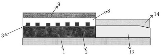
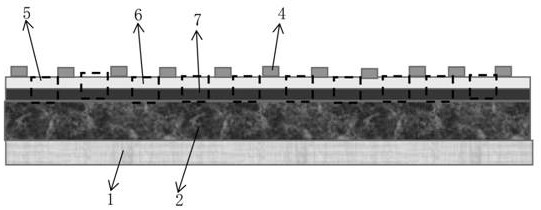
[0079] Step 1: See image 3 , the active layer 2 is deposited on the InP substrate 1 using metal-organic vapor phase epitaxy, and the grating layer 3 is deposited on the active layer 2 (the grating layer 3 includes a layer of InGaAsP layer 7 and a layer of first InP layer 6), and on the first InP Deposit mask 4 on layer 6, use photolithography technology to leak out the first etching region 5 that needs to be etched, and then use dry etching technology to etch InGaAsP layer 7 to the first InP layer 6 at the bottom, thereby making InGaAsP material The grating structure, that is, the grating layer 3 is obtained.

[0080] Step 2: see Figure 4 , using metal-organic vapor phase epitaxy to deposit a second InP layer 8 on the grating structure to fill up the etched area between the grating structures and ensure the stability of the grating structure.

[0081] Step Three: See Figure 5 , deposit a mask layer 9 on the product obtained in step 2, and use photolithography to place Si...

Embodiment 2

[0086] Step 1: See image 3 On the InP substrate 1, the active layer 2 is deposited by metal-organic vapor phase epitaxy, and the grating layer 3 (including a layer of InGaAsP layer 7 and a layer of the first InP layer 6 ) is deposited on the active layer. Mask 4, using photolithography technology to leak out the first etching region 5 that needs to be etched, and then using dry etching technology to etch the InGaAsP layer 7 to the first InP layer 6 at the bottom, thereby making a grating structure of InGaAsP material, That is, the grating layer 3 is obtained.

[0087] Step 2: see Figure 4 , using metal-organic vapor phase epitaxy to deposit a second InP layer 8 on the grating structure to fill up the etched area between the grating structures and ensure the stability of the grating structure.

[0088] Step Three: See Figure 5 , deposit a mask layer 9 on the product obtained in step 2, and use photolithography to place SiO 2 Etched into a rectangular structure, the SiO ...


PUM


Abstract

The invention discloses an aluminum quantum well laser and a preparation method thereof. The preparation method comprises the following steps: using ammonium polysulfide solution to treat oxides on the etching surface, and forming a sulfide protective layer; using metal-organic vapor phase deposition on the surface of an InP substrate The waveguide layer and the third InP layer are grown sequentially. During the temperature rise process before metal-organic vapor phase epitaxy growth, the etched surface is baked to desorb the sulfur atoms of the sulfide protective layer, and the sulfur element is generated and sublimated with the carrier gas. Compared with the traditional passivation technology, the invented process for solving the oxidation problem of the etching surface of the aluminum-containing quantum well laser has low cost, simple process and strong stability.

Description

technical field [0001] The invention belongs to the technical field of semiconductor laser chip preparation, and in particular relates to an aluminum quantum well laser and a preparation method thereof. Background technique [0002] Distributed feedback lasers (DFB) have the characteristics of high side mode suppression ratio, narrow linewidth, high modulation rate, and dynamic single longitudinal mode. With the gradual commercialization of 5G, distributed feedback lasers will bear the brunt of becoming the main light source. There are two kinds of materials used in the active region of DFB lasers, one is InGaAsP material and the other is AlInGaAs material. The main difference between the two material systems is the distribution of conduction band and valence band offset. In phosphorus system, The energy shift of the quantum well potential in the conduction band is smaller than that in the valence band, while in the aluminum system, the situation is just the opposite. There...

Claims


Application Information

Patent Timeline
Patent Type & Authority Patents(China)
IPC IPC(8): H01S5/12H01S5/343
CPCH01S5/12H01S5/3432
Inventor 张海超穆瑶师宇晨李马惠潘彦廷
Owner SHANXI YUANJIE SEMICONDUCTOR TECH CO LTD
Why Eureka
Try Eureka