Aluminum quantum well laser device and preparation method thereof
A laser and aluminum quantum technology, which is applied in the direction of lasers, phonon exciters, laser components, etc., can solve the problem of poor etching surface performance
- Summary
- Abstract
- Description
- Claims
- Application Information
AI Technical Summary
Problems solved by technology
Method used
Image
Examples
preparation example Construction
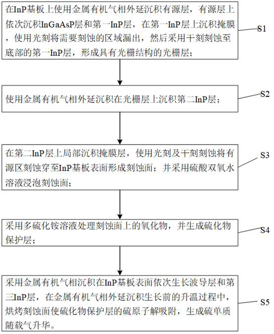
[0052] like figure 1 Shown, the first object of the present invention is to provide a kind of preparation method of aluminum quantum well laser, comprises the following steps:
[0053] Step 1: Deposit the active layer on the InP substrate using metal-organic vapor phase epitaxy, deposit an InGaAsP layer and a first InP layer on the active layer, and deposit a mask layer on the first InP layer. The area to be etched is leaked out, and then the first InP layer at the bottom is etched by dry etching technology, so as to form a grating structure of InGaAsP material, that is, the grating layer 3 is obtained.
[0054] Further, dry etching uses inductively coupled plasma equipment, and the etching gas source is Cl 2 Gas, H 2 Body and Ar body, Cl 2 Gas, H 2 The flow rates of the bulk and the Ar bulk were 20 sccm, 15 sccm and 30 sccm, respectively. The material of the mask layer is photoresist.
[0055] Step 2: Depositing a second InP layer on the grating structure using metalorg...
Embodiment 1
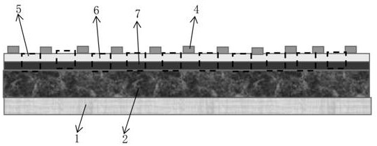
[0079] Step 1: See image 3 , the active layer 2 is deposited on the InP substrate 1 using metal-organic vapor phase epitaxy, and the grating layer 3 is deposited on the active layer 2 (the grating layer 3 includes a layer of InGaAsP layer 7 and a layer of first InP layer 6), and on the first InP Deposit mask 4 on layer 6, use photolithography technology to leak out the first etching region 5 that needs to be etched, and then use dry etching technology to etch InGaAsP layer 7 to the first InP layer 6 at the bottom, thereby making InGaAsP material The grating structure, that is, the grating layer 3 is obtained.
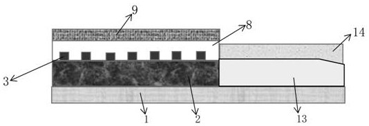
[0080] Step 2: see Figure 4 , using metal-organic vapor phase epitaxy to deposit a second InP layer 8 on the grating structure to fill up the etched area between the grating structures and ensure the stability of the grating structure.
[0081] Step Three: See Figure 5 , deposit a mask layer 9 on the product obtained in step 2, and use photolithography to place Si...
Embodiment 2
[0086] Step 1: See image 3 On the InP substrate 1, the active layer 2 is deposited by metal-organic vapor phase epitaxy, and the grating layer 3 (including a layer of InGaAsP layer 7 and a layer of the first InP layer 6 ) is deposited on the active layer. Mask 4, using photolithography technology to leak out the first etching region 5 that needs to be etched, and then using dry etching technology to etch the InGaAsP layer 7 to the first InP layer 6 at the bottom, thereby making a grating structure of InGaAsP material, That is, the grating layer 3 is obtained.
[0087] Step 2: see Figure 4 , using metal-organic vapor phase epitaxy to deposit a second InP layer 8 on the grating structure to fill up the etched area between the grating structures and ensure the stability of the grating structure.
[0088] Step Three: See Figure 5 , deposit a mask layer 9 on the product obtained in step 2, and use photolithography to place SiO 2 Etched rectangular structure, using dry etchin...
PUM
| Property | Measurement | Unit |
|---|---|---|
| Thickness | aaaaa | aaaaa |
Abstract
Description
Claims
Application Information


