Photovoltaic green building material and preparation method thereof
A technology for green building materials and photovoltaics, applied in the field of photovoltaic green building materials and their preparation, can solve the problems of easy occurrence of short circuits, chipped cells, and reducing the overall aesthetics of photovoltaic building materials.
- Summary
- Abstract
- Description
- Claims
- Application Information
AI Technical Summary
Problems solved by technology
Method used
Image
Examples
preparation example Construction
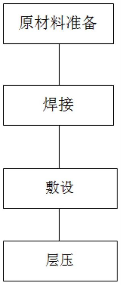
[0046] A method for preparing a photovoltaic green building material, comprising the following steps:
[0047] Obtain the first temperature of the glass front, back plate, and PVB glue, and keep the first temperature at 25°C-30°C;
[0048] Weld single crystal cells into cell strings;
[0049] The battery string is laid on the backplane, and the glass front and backplane are combined and laminated with PVB glue to prepare photovoltaic green building materials. The second temperature of the lamination process is 25°C-30°C, The time interval of the combination process shall not exceed 5 minutes.
[0050] In the process of welding the monocrystalline cells into the battery string, it also includes keeping the length of the inter-chip welding strips consistent, and at the end of the welding, the welding tool extends to the outside of the monocrystalline cells; the time interval is 1-5 minutes.
[0051] The assembling process also includes fixing the non-terminal welding strips o...
Embodiment 1
[0053] Embodiment 1: The specific preparation process of the preparation method of a kind of photovoltaic green building material that the present invention provides is:
[0054] 1. Raw material preparation: heat preservation of glass and PVB before production, and the ambient temperature is 25°C-30°C.
[0055] 2. Welding:
[0056] Pay attention to the welding method when soldering. At the end, it should extend to the outside of the battery and lift the tip of the soldering iron.
[0057] During the soldering process, pay attention to tin spots and tin bumps, and smooth them with a soldering iron in time. Pay attention to open welding when welding, inspect while welding, and repair in time.
[0058] When soldering, pay attention to the length of the inter-chip welding strips to avoid S-bends in the inter-chip welding strips, resulting in unqualified appearance and broken cells.
[0059] When welding, pay attention to the connection method of the ribbon and weld according to...
PUM
 Abstract
Description
Claims
Application Information


