Diamond nuclear detector based on hydrogen-oxygen terminal full-vertical structure and preparation method
A vertical structure, nuclear detector technology, applied in the field of semiconductor technology, can solve the problems of large diamond surface work function, surface movable ion leakage, unfriendly environment, etc., and achieves suppression of surface leakage, high energy collection efficiency, high energy deposition. Effect
- Summary
- Abstract
- Description
- Claims
- Application Information
AI Technical Summary
Problems solved by technology
Method used
Image

Examples
Embodiment 1
[0044] The basic working principle of the nuclear detector is that the nuclear radiation interacts with the detector material, and the energy is deposited in the nuclear detector body to generate electron-hole pairs. After these charges are collected by the electric field on the electrodes at both ends of the nuclear detector, they are generated in the external circuit. Electrical signal, nuclear radiation is detected if the electrical signal of the nuclear detector after the radiation is incident is significantly higher than the background dark signal (dark current) when no radiation is incident. In addition, the contact between the nuclear detector material and the electrode should not produce high contact resistance, and should not produce obvious nonlinear characteristics. The external electric field should be applied to the energy deposition area as much as possible, thereby reducing the "dead zone" , to improve the charge collection efficiency, so that the nuclear detecto...
Embodiment 2
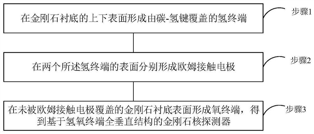
[0070] See Figure 2a-2e , Figure 2a-2e It is a process schematic diagram of a hydrogen-oxygen terminal-based diamond nuclear detector provided by an embodiment of the present invention. On the basis of the above-mentioned embodiments, this embodiment will introduce the process flow of the present invention in more detail. The method includes:
[0071] S01: Select the substrate. Such as Figure 2a As shown, a certain thickness of single crystal diamond material 001 is selected as the substrate material, and the inorganic and organic cleaning are performed sequentially.
[0072] S02: Hydrogen terminal preparation. Such as Figure 2b As shown, at a temperature of 700-950 ° C, the diamond substrate 001 is placed in hydrogen plasma for microwave plasma chemical vapor deposition reaction for 5-30 minutes, cooled to room temperature in a hydrogen atmosphere, and the upper and lower surfaces of the diamond substrate 001 Formation of hydrogen terminal 002 covered by carbon-hydr...
Embodiment 3
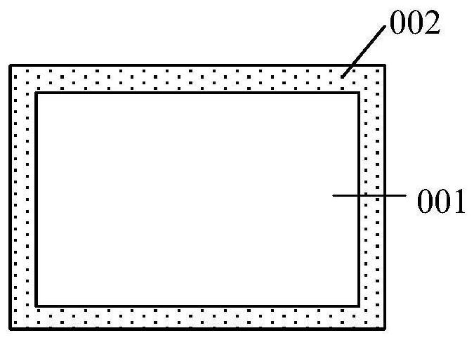
[0081] See image 3 and Figure 4 , image 3 It is a schematic diagram of the three-dimensional structure of a diamond nuclear detector based on a hydrogen-oxygen terminal full vertical structure provided by an embodiment of the present invention (the oxygen terminal on the side surface of the diamond substrate 001 is at image 3 not shown in); Figure 4 It is a schematic cross-sectional view of a diamond nuclear detector based on a hydrogen-oxygen terminal full vertical structure provided by an embodiment of the present invention. As shown in the figure, this embodiment provides a diamond nuclear detector based on a hydrogen-oxygen terminal full vertical structure, including: a diamond substrate 001, a hydrogen terminal 002 located on the upper and lower surfaces of the diamond substrate 001, and a hydrogen terminal located on the surface 002 of the hydrogen terminal. The ohmic contact electrode 003, and the oxygen terminal 004 located on the surface of the diamond substrate...
PUM
| Property | Measurement | Unit |
|---|---|---|
| Thickness | aaaaa | aaaaa |
Abstract
Description
Claims
Application Information