
Patsnap Eureka
For R&D, Patsnap Eureka makes reading and utilizing patents & technical documents easy.
Patsnap Eureka AIR
Designed for self-driven R&D workflows. Generate viable solutions, solve complex R&D challenges, empower your innovation with AI.

Patsnap Eureka Materials
Designed for material experts only. Revolutionize your material R&D, from search, analyze, to developing new materials.

TechResearch
Generate reliable direction feasibility study reports for your R&D in just a few steps.

TechSeek
Discover and master advanced knowledge NOW. Basics, ideas, possibilities, all at once.

TechMind
As an expert in R&D Theories, TechMind can generates customized viable solutions instantly.

TechRisk
Analyze your overall solution with one click, know your potential R&D risks in advance.

TechMonitor
Get weekly tech updates, stay abreast of the latest tech innovations and key insights.
Ceramic-based double-sided RDL 3D packaging method and structure
A packaging method and packaging structure technology, applied in electrical components, electrical solid devices, circuits, etc., can solve electromagnetic shielding design, reliability, flexibility, cost production cycle, system heat dissipation short board, difficult to achieve large-scale system integration , affecting system performance and other issues, to achieve the effect of shortening physical distance, reducing transmission loss, and reducing system thermal resistance
- Summary
- Abstract
- Description
- Claims
- Application Information
AI Technical Summary
Problems solved by technology
Method used
Image

Examples
Embodiment 1
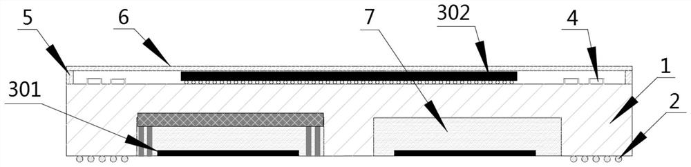
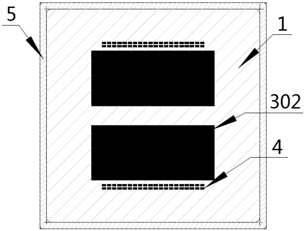
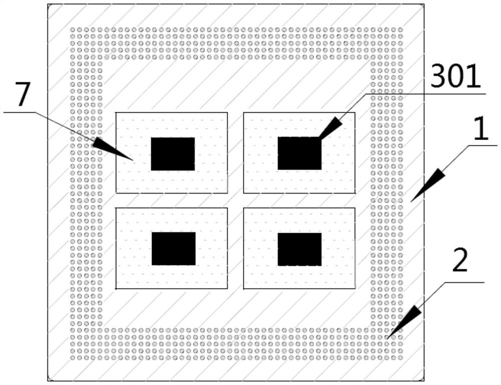
[0037] Example 1, see Figure 1-5 , a ceramic-based double-sided RDL 3D packaging structure, including a ceramic substrate 9 with a multi-layer wiring structure, and the interior of the ceramic substrate 9 is electrically vertically interconnected through thick-film TCV vias 11; the front of the ceramic substrate 9 is prepared with a front multi-layer Thin film RDL layer 14, electronic devices such as active chips 2 302 and passive devices 4 are installed on the front multilayer thin film RDL layer 14, metal ring frame 5 can be assembled by gold tin / silver copper welding, and metal ring frame 5 is welded The cover plate 6 realizes airtight packaging. The back side of ceramic substrate 9 offers at least one cavity, and the inside of cavity is also provided with electronic device, and electronic device can be active chip-301 here, also can be the combination of active chip-301 and passive device, active chip The number of one 301 is designed according to the demand, and the mod...
Embodiment 2
[0039]Embodiment 2, for the cavity, a thick-film TCV through hole 11 can be provided inside the cavity for grounding, or a composite metal layer 15 can be printed on the bottom surface of the cavity to realize a metal interconnection structure. According to design requirements, the cavity can also be designed as an electromagnetic shielding cavity. In the electromagnetic shielding cavity, the composite metal layer 15 and the thick-film TCV through-holes 11 exist at the same time, and there are at least four thick-film TCV through-holes 11 arranged around the active chip one 301 . Thus, the thick-film TCV through-hole 11 and the composite metal layer 15 form an electromagnetic shielding structure to protect the active chip 1 301 .
Embodiment 3
[0040] Embodiment 3, above-mentioned encapsulation structure is made by the encapsulation method of following steps, as Figure 7 As shown, the specific steps are as follows:
[0041] Step 1: preparing a ceramic substrate with a cavity structure on the back;
[0042] Specifically, step 1 includes the following steps:
[0043] Step 1.1: Al 2 o 3 / AlN slurry casting into Al 2 o 3 / AlN raw ceramic belt, according to the design requirements for Al 2 o 3 / AlN raw porcelain tape for cutting and punching.
[0044] Step 1.2: According to the design requirements, print a composite metallization pattern 10 on each layer of green ceramic tape, and at the same time fill the punched holes with metals such as Au, Ag, W, WCu, WTi, MoCu to form thick film TCV through holes 11 , according to the design requirements, in the cavity on the back of the green ceramic tape, print the composite metal layer 15 or make the thick film TCV through hole 11 or both. When performed at the same time...
PUM
 Abstract
Description
Claims
Application Information
 - R&D Engineer
- R&D Manager
- IP Professional
- Industry Leading Data Capabilities
- Powerful AI technology
- Patent DNA Extraction
Browse by: Latest US Patents, China's latest patents, Technical Efficacy Thesaurus, Application Domain, Technology Topic, Popular Technical Reports.
© 2024 PatSnap. All rights reserved.Legal|Privacy policy|Modern Slavery Act Transparency Statement|Sitemap|About US| Contact US: help@patsnap.com