MEMS silicon-based cavity circulator/isolator circuit film structure and preparation method
A circulator and isolator technology, applied in the field of MEMS silicon-based cavity circulator/isolator circuit film layer structure and preparation, can solve the problems of reducing the resistivity of high-resistance silicon, increasing device insertion loss, and large conductor loss, etc. , to achieve the effect of reducing insertion loss, reducing conductor loss and low loss requirements
- Summary
- Abstract
- Description
- Claims
- Application Information
AI Technical Summary
Problems solved by technology
Method used
Image
Examples
Embodiment 1
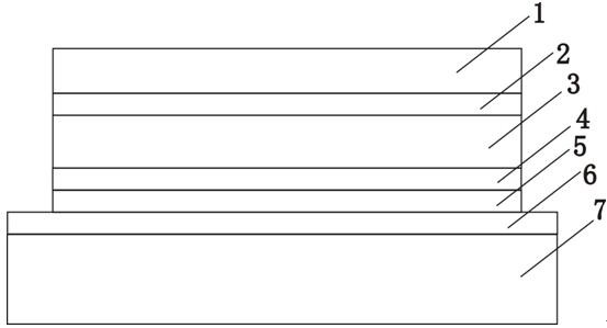
[0034] see figure 1 , a MEMS silicon-based cavity circulator / isolator circuit film structure, which includes a gold film layer 1, a barrier film layer 2 (titanium film), a copper film layer 3, and a tantalum nitride support film layer 4 from top to bottom , base film layer 5 (chromium film), isolation film layer 6 (silicon dioxide film) and high resistance silicon layer 7;
[0035] The preparation method is as follows:
[0036] (1) Marking and cleaning two high-resistance silicon layers 7;
[0037] (2) Uniformly oxidize a layer of 300nm thick silicon dioxide film on the front and back of the high resistance silicon layer 7 as the isolation film layer 6;
[0038] (3) Magnetron sputtering is used to sputter a layer of metal chromium thin film as the base layer 5, room temperature sputtering, sputtering power 180W, chromium film thickness 30nm;
[0039] (4) Put the silicon wafer into a box furnace for vacuum annealing, the annealing temperature is 250°C, and the annealing time...
Embodiment 2
[0049] A MEMS silicon-based cavity circulator / isolator circuit film structure, which includes gold film layer 1, barrier film layer 2 (titanium film), copper film layer 3, tantalum nitride support film layer 4, Primer film layer 5 (titanium film), isolation film layer 6 (silicon dioxide film) and high resistance silicon layer 7;
[0050] The preparation method is as follows:
[0051] (1) Marking and cleaning two high-resistance silicon layers 7;
[0052] (2) Uniformly oxidize a layer of 180nm thick silicon dioxide film on the front and back of the high-resistance silicon layer 7;
[0053] (3) Magnetron sputtering is used to sputter a layer of metal titanium thin film as the base layer 5, room temperature sputtering, sputtering power 180W, titanium film thickness 50nm;
[0054] (4) Sputter a layer of copper film on the titanium film, the sputtering temperature is 400°C, the sputtering power is 900W, and the thickness of the copper film is 4000nm;
[0055] (5) sputtering a la...
Embodiment 3
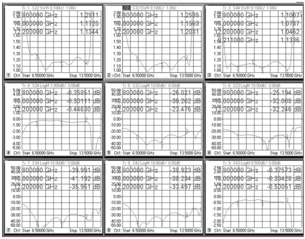
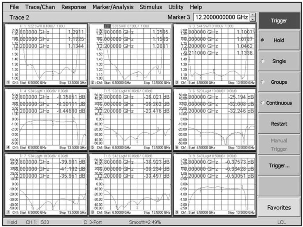
[0062] Compared with Example 2 in this example, only in step (2) is "a metal titanium layer after uniformly evaporating a layer of 50nm metal titanium layer on the front and back of the high-resistance silicon layer 7, and the rest are the same as in Example 1, using the obtained film layer structure, the electrical performance test was carried out on the assembled 8-12GHz MEMS silicon-based isolator device, and the result was that the insertion loss ILMAX=0.58dB of the single-section device was 0.17dB lower than that of the MEMS isolator with the chromium / gold structure in the same frequency band.
PUM
| Property | Measurement | Unit |
|---|---|---|
| thickness | aaaaa | aaaaa |
| thickness | aaaaa | aaaaa |
| thickness | aaaaa | aaaaa |
Abstract
Description
Claims
Application Information


