Preparation method of modified silicon wafer loading material and application of modified silicon wafer loading material in cell culture

A technology for loading materials and silicon wafers, applied in cell culture supports/coatings, general culture methods, biochemical equipment and methods, etc. Adhesion and other problems, to achieve the effect of favorable adhesion growth, industrialized large-scale production, and multi-loading area

Pending Publication Date: 2021-08-24
SUN YAT SEN UNIV
View PDF7 Cites 2 Cited by
  • Summary
  • Abstract
  • Description
  • Claims
  • Application Information

AI Technical Summary

Problems solved by technology

[0004] At present, many bioreactors use polished silicon wafers as the load material for cell culture, but because polished silicon wafers are hydrophobic materials, they are directly used for cell culture, which is not conducive to cell adhesion, and in the dynamic culture mode of the reactor, Smooth silicon wafers are easy to cause cells to fall off, which is not conducive to cell adhesion and growth
At the same time, polished silicon wafers can only provide a single-layer culture mode. For cells with complex growth environments (such as mesenchymal stem cells), they cannot simulate the complex niche environment of cell growth, which will affect the in vitro expansion of cells. ability and differentiation ability after multiple passages, and the limited seeding area cannot effectively expand a sufficient number of high-quality cells in a short period of time

Method used


Image

  • Preparation method of modified silicon wafer loading material and application of modified silicon wafer loading material in cell culture
  • Preparation method of modified silicon wafer loading material and application of modified silicon wafer loading material in cell culture
  • Preparation method of modified silicon wafer loading material and application of modified silicon wafer loading material in cell culture

Examples


Embodiment 1

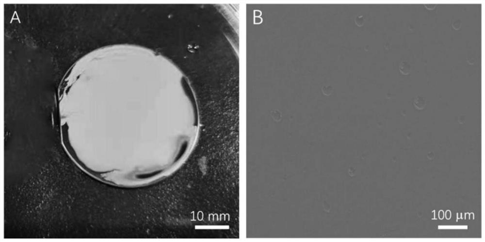
[0032] The preparation of embodiment 1 modified silicon chip support material

[0033] (1) Weigh 5g of NaOH solid, dissolve it in 100mL of 75% ethanol solution to prepare alkali washing solution, place silicon chip (circular silicon chip with a diameter of 32mm) in the above alkali washing solution for 3h, dry and place Sterilize under high temperature and high pressure at 120°C for 30 minutes, and put it in an ultra-clean bench for use after sterilization.

[0034](2) Measure 9mL of 30% hydrogen peroxide and 21mL of concentrated sulfuric acid with a clean graduated cylinder, drain with a glass rod, slowly add hydrogen peroxide into the concentrated sulfuric acid solution, and stir while adding, to obtain concentrated sulfuric acid and hydrogen peroxide Soak the silicon chip treated in step (1) in the above mixed solution of concentrated sulfuric acid and hydrogen peroxide, treat for 3h, then rinse the silicon chip with deionized water, 10mL each time, rinse 3 times, 1 minute...

Embodiment 2

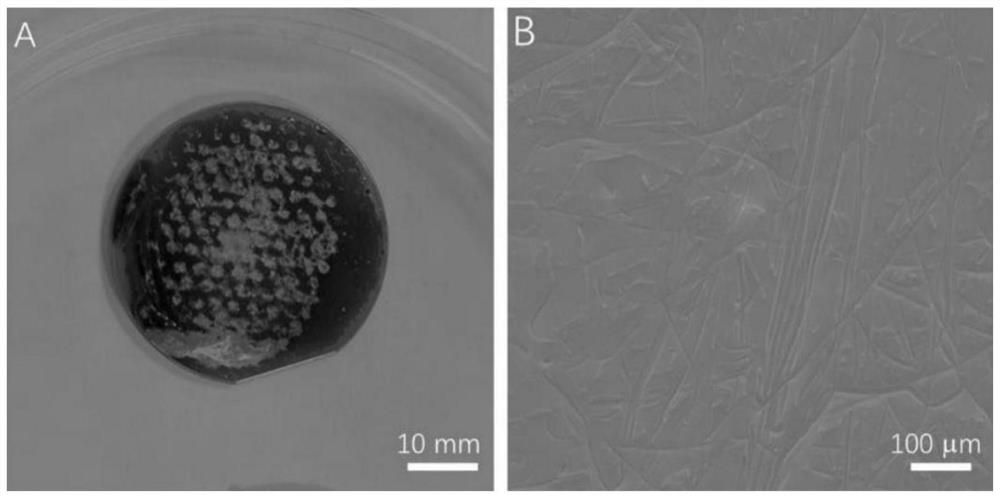
[0040] The preparation of embodiment 2 modified silicon chip support materials

[0041] Steps (1)-(5) are the same as in Example 1;

[0042] (6) Soak the dried silicon wafer in 90% ethanol solution at 80°C for 60 minutes, then place a clean PP non-woven fabric in a glass dish, and press the gelatin side of the silicon wafer on the PP non-woven fabric. Spin cloth, and use 500g weight to gently press down on the silicon wafer. After 24 hours, gently uncover the PP film, wash the silicon wafer with 5mL of absolute ethanol, wash 3 times in total, 1 minute each time, and then soak the silicon wafer in an absolute ethanol solution containing 0.25% glutaraldehyde for 30 minutes After treatment, wash with normal temperature absolute ethanol or dioxane (first wash 3 times with 5mL normal temperature absolute ethanol, 1 minute each time, then wash 3 times with 5mL normal temperature dioxane, 1 minute each time) , and finally placed in an oven at 37°C for drying treatment, and stored i...

Embodiment 3

[0044] The preparation of embodiment 3 modified silicon chip support materials

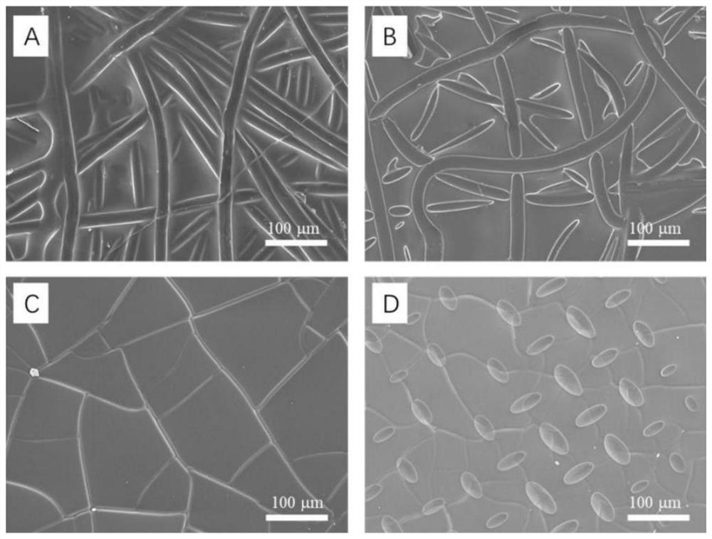
[0045] The preparation method is the same as in Example 2, the difference is that the PP film is replaced by PET commercial carrier, PET non-woven fabric, sampling screen, cell screen, and a gelatin coating with a special topological structure is prepared on the surface of the silicon chip , to prepare modified silicon wafer loading materials with various special topological structures.

[0046] The microscopic morphology of the prepared modified silicon wafer-loaded materials with various special topological structures (PET non-woven fabric, PP non-woven fabric, sampling screen, cell screen) was observed. The SEM images are as follows: Figure 5 Shown: It can be seen that each group of embossed patterns is a topological structure with a special shape, in which groups A and B form a fiber structure with a sense of hierarchy, while C and D are patterns prepared through a screen, similar to those fo...


PUM

PropertyMeasurementUnit
diameteraaaaaaaaaa

Abstract

The invention belongs to the technical field of cell culture loading materials, and particularly relates to a preparation method of a modified silicon wafer loading material and application of the modified silicon wafer loading material in cell culture. According to the invention, gelatin macromolecules are loaded on the surface of a polished silicon wafer, and then a gelatin coating with micropores is formed on the surface of the silicon wafer by using a lyotropic phase separation method or a gelatin coating with a specific three-dimensional topological structure is prepared by using a micro-pattern printing technology; and thus, the modified silicon wafer cell loading material with a micropore or fiber topological structure on the surface is prepared. The modified silicon wafer overcomes the limitation of the hydrophobicity of a silicon wafer material and a single-layer culture mode, not only has good biocompatibility, but also is more beneficial to the adhesion and growth of cells due to the three-dimensional gelatin coating structure of the modified silicon wafer, and can effectively simulate the three-dimensional environment of cell growth; meanwhile, under the limited volume, a larger loading area can be provided, and the modified silicon wafer loading material is suitable for being used as a large-scale cell culture material.

Description

technical field [0001] The invention belongs to the technical field of cell culture loading materials, and in particular relates to a preparation method of a modified silicon chip loading material and its application in cell culture. Background technique [0002] Cell culture is an essential process in bioengineering technology research. Cell types are divided into attached type and suspension type according to the characteristics of whether they are attached to the support or not. Cells that grow only by attaching to the surface of the support are called attached cells; cells that do not grow on the support are called suspension cells. Most animal cells have the habit of growing on the wall. Therefore, when culturing in vitro, it is usually necessary to provide a support for its growth. This support refers to the cell culture carrier often referred to by those skilled in the art. In the process of cell culture, cell culture carrier plays a very important role in the regul...

Claims


Application Information

Patent Timeline
Patent Type & Authority Applications(China)
IPC IPC(8): C12N5/00C04B41/48C09D189/00
CPCC12N5/0068C04B41/48C09D189/00C12N2533/54C12N2533/10
Inventor 龚逸鸿曹聪罗语溪李燕叶浩刘海东李晋泽符童朱应欧
Owner SUN YAT SEN UNIV
Why Eureka
Try Eureka