
A trench type Schottky device and its manufacturing method

A manufacturing method and trench-type technology, applied in semiconductor/solid-state device manufacturing, semiconductor devices, electrical components, etc., can solve problems such as leakage, and achieve the effect of avoiding direct contact and high matching.

Active Publication Date: 2022-04-08
JIANGSU HAIDONG SEMICON TECH CO LTD
View PDF26 Cites 0 Cited by
  • Summary
  • Abstract
  • Description
  • Claims
  • Application Information

AI Technical Summary

Problems solved by technology

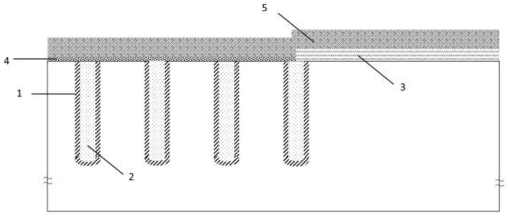
[0004] In the above processes of the prior art, it is necessary to precisely control the etching depth of the contact hole, the intra-chip uniformity of the etching rate, and the thickness of the barrier; there is a situation where the contact metal directly contacts the silicon and causes leakage ( figure 1 )

Method used


Image

  • A trench type Schottky device and its manufacturing method
  • A trench type Schottky device and its manufacturing method
  • A trench type Schottky device and its manufacturing method

Examples


Embodiment Construction

[0040] The present invention will be described in further detail below in conjunction with examples and specific implementation methods.

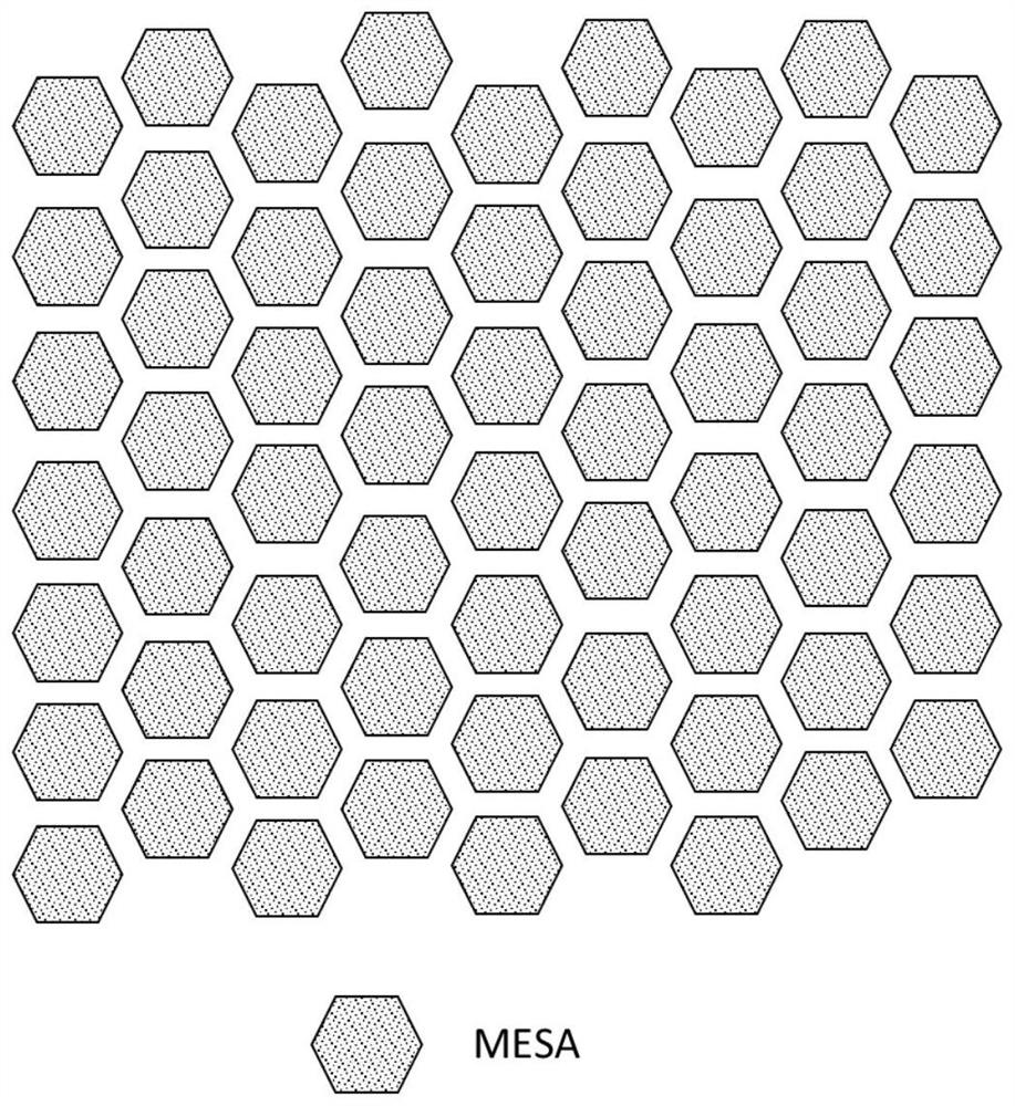
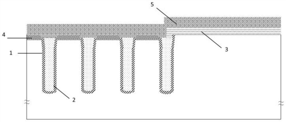
[0041] Such as figure 2 As shown, a trench-type Schottky device, its structure is a trench-type Schottky diode structure with a hexagonal cell structure, such as image 3 As shown, the topography of the trench has an oblique angle, and the metal interface of the barrier layer is lower than the interface of the contact metal layer in the vertical direction.

[0042] It is verified by experiments that the present invention adopts the hexagonal cell structure to maximize area utilization and ensure the best adaptability to subsequent technological processes. And the HDP process is added after the barrier metal is formed to ensure that the interface of the barrier metal is always 0.1um~0.3um lower than the interface of the contact metal in the vertical direction, which can avoid the leakage channel caused by the direct contact between the con...


PUM

PropertyMeasurementUnit
thicknessaaaaaaaaaa

Abstract

The invention relates to a trench type Schottky device and a manufacturing method thereof. The structure is that the cell structure is hexagonal, the top of the trench is inclined, and the metal interface of the barrier layer is lower than the interface of the contact metal layer in the vertical direction. Methods: 1) growing an oxide layer on the epitaxial wafer; 2) etching the trench by photolithography; 3) generating gate oxide in the trench; 4) filling the trench with polysilicon; 5) etching back the polysilicon; 6) removing the oxide layer by wet method; 7 ) High temperature thermal oxidation; 8) SiN deposition, ILD silicon dioxide layer deposition; 9) Schottky contact hole photolithography, wet silicon dioxide removal; 10) SiN / thermal oxide layer dry etching; 11) Schottky barrier metal sputtering; 12) barrier metal alloy / barrier metal removal; 13) HPD deposition; 14) contact metal sputtering; 15) contact metal photolithography; 16) back gold thinning. Advantages: maximize the utilization of the cell area, and have a high degree of matching with the process flow; the barrier metal is better accumulated inside the trench; avoid leakage channels.

Description

technical field [0001] The invention relates to a trench type Schottky device and a manufacturing method thereof, in particular to a trench type Schottky diode structure and a manufacturing method thereof. Background technique [0002] Trench-type Schottky diodes are common power devices for semiconductors, which were invented by utilizing the MOS effect of metal-semiconductor-silicon. Its main feature is that as the reverse voltage increases, the trenches are pinched off in advance through the MOS effect, and the electric field strength drops to zero before reaching the silicon surface, avoiding breakdown on the surface and improving the blocking ability. [0003] In the prior art, the manufacturing process of trench-type Schottky diodes is as follows: growing oxide layer as a hard mask layer-trench photolithography-trench etching-polysilicon filling-polysilicon back-etching-contact hole photolithography-contact Hole etching - barrier metal sputtering - barrier metal alloy...

Claims


Application Information

Patent Timeline
Patent Type & Authority Patents(China)
IPC IPC(8): H01L29/872H01L21/329
CPCH01L29/66143H01L29/8725
Inventor 夏华忠诸建周李健黄传伟
Owner JIANGSU HAIDONG SEMICON TECH CO LTD
Learn More