

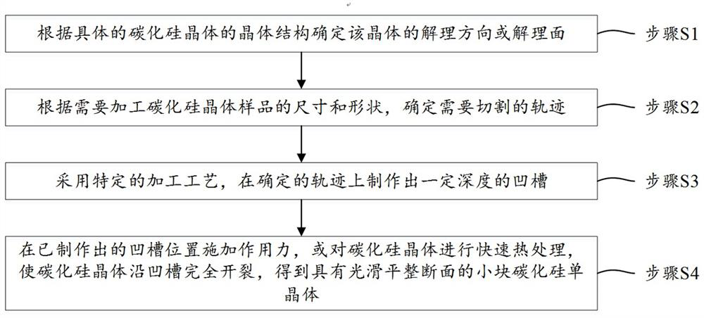
Cutting method of silicon carbide crystal
A cutting method and silicon carbide technology, applied in chemical instruments and methods, crystal growth, single crystal growth and other directions, can solve the problems of rough cutting surface, low efficiency, high cost, small cutting loss, simple cutting process, and improved utilization. rate effect
- Summary
- Abstract
- Description
- Claims
- Application Information
AI Technical Summary
Problems solved by technology
Method used
Image

Examples
specific Embodiment 1
[0057] Cut a 4-inch cylindrical 4H-SiC (α-SiC) single crystal sample into small pieces with neat and smooth sections by laser cutting process, and observe its internal defects. The specific steps are as follows:
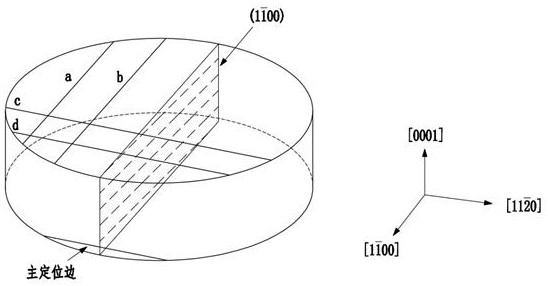
[0058] (1) Use X-ray crystal orientation instrument to determine the cleavage direction of 4H-SiC: and mark with a marker pen;
[0059] (2) Make parallel to the defect position of the sample The straight line of the direction and marked;
[0060] (3) Place the sample on the sample stage of the laser cutting machine, set the trajectory of the laser scanning to coincide with the marking line in step (2), set the width of the laser beam to 0.03mm, turn on the laser, and make the laser beam cut along the marking line , stop when the cutting depth reaches 0.2mm, and prepare grooves along the cleavage direction;
[0061] (4) Put the sample into the heating furnace and rapidly raise the temperature to 600°C, and keep the heating rate at 60°C / S. Thermal stress is gene...
specific Embodiment 2
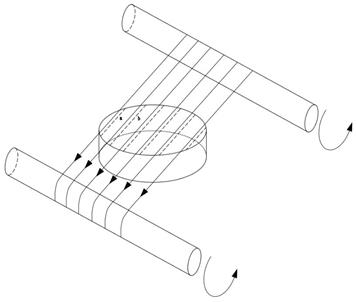
[0064] The 6-inch cylindrical 6H-SiC (α-SiC) single crystal sample is cut into a rough silicon carbide gemstone with a neat and smooth cross-section by the wire cutting process. The specific steps are as follows:
[0065] (1) Use X-ray crystal orientation instrument to determine the cleavage direction of 6H-SiC: and Use a marker to make straight marks;
[0066] (2) Make parallel to the defect position of the sample and A plurality of straight lines in the direction are marked, and the distance between the parallel lines is determined according to the size of the silicon carbide gem, and the present embodiment adopts a spacing of 8mm;
[0067] (3) Place the sample on the sample table of the multi-wire cutting machine, adjust the position of the sample so that the direction of the reciprocating motion (cutting) of the steel wire coincides with the marking line, set the depth to 0.3mm, start the multi-wire cutting machine, and prepare Multiple grooves along the cleaving d...
PUM
| Property | Measurement | Unit |
|---|---|---|
| refractive index | aaaaa | aaaaa |
| Mohs hardness | aaaaa | aaaaa |
Abstract
Description
Claims
Application Information