Monolithic integrated edge emitting laser and preparation method thereof

An edge-emitting laser and monolithic integration technology, which is applied to lasers, laser components, semiconductor lasers, etc., can solve the problems of low system stability and bulky laser radar system

Active Publication Date: 2021-09-10
INST OF SEMICONDUCTORS - CHINESE ACAD OF SCI
View PDF7 Cites 0 Cited by
  • Summary
  • Abstract
  • Description
  • Claims
  • Application Information

AI Technical Summary

Problems solved by technology

Therefore, the volume of the entire lidar system is relatively large, and the stability of the system is relatively low

Method used


Image

  • Monolithic integrated edge emitting laser and preparation method thereof
  • Monolithic integrated edge emitting laser and preparation method thereof
  • Monolithic integrated edge emitting laser and preparation method thereof

Examples


Embodiment 1

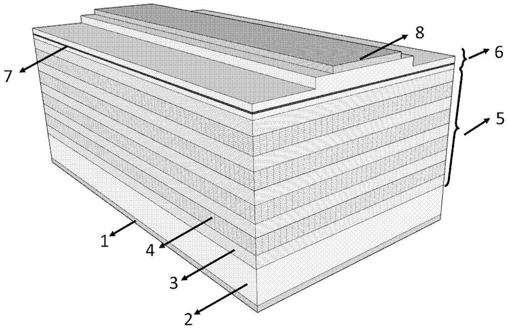
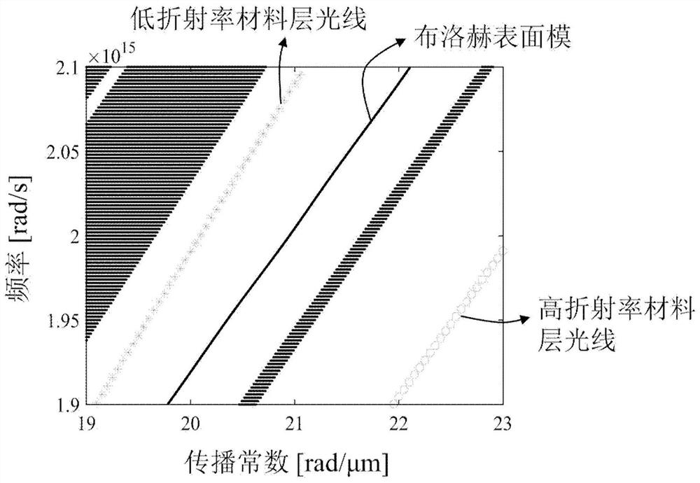
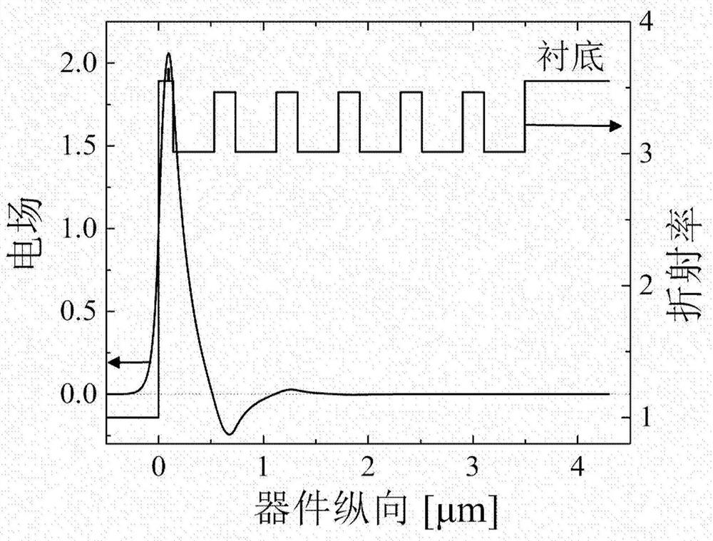
[0058] In this embodiment, the monolithic integrated edge-emitting laser operates at a wavelength of 940 nm and is based on gallium arsenide (GaAs) material.

[0059] The structure of monolithic integrated edge-emitting laser is as follows figure 1 As shown: the first electrode 1 is the negative electrode, and the material is AuGeNiAu; the second electrode 8 is the positive electrode, and the material is TiPtAu; the material of the substrate 2 is n-type GaAs; the low refractive index material layer 3 is n-type Al 0.9 Ga 0.1 As layer, the thickness is 334nm, the first high refractive index material layer 4 is n-type Al 0.12 Ga 0.88 The As layer has a thickness of 157nm. The low-refractive-index material layer 3 and the first high-refractive-index material layer 4 are periodically alternately grown in 5.5 groups during material epitaxy, forming a multilayer structure 5 similar to a Bragg mirror structure. The multilayer structure 5 is formed on the substrate, and the multilay...

Embodiment 2

[0064] In this embodiment, the monolithic integrated edge-emitting laser operates at a wavelength of 940 nm and is based on gallium arsenide (GaAs) material.

[0065] The structure of monolithic integrated edge-emitting laser is as follows Figure 5 As shown: the first electrode 1 is the negative electrode, and the material is AuGeNiAu; the second electrode 8 is the positive electrode, and the material is TiAu; the material of the substrate 2 is n-type GaAs; the low-refractive index material layer 3 is n-type Al 0.9 Ga 0.1 As layer, the thickness is 334nm, the first high refractive index material layer 4 is n-type Al 0.12 Ga 0.88 The As layer has a thickness of 157nm. The low-refractive-index material layer 3 and the first high-refractive-index material layer 4 are periodically alternately grown in 5.5 groups during material epitaxy, forming a multilayer structure 5 similar to a Bragg mirror structure. The multilayer structure 5 is formed on the substrate, and the multilaye...

Embodiment 3

[0067] In this embodiment, the monolithic integrated edge-emitting laser operates at a wavelength of 940 nm and is based on gallium arsenide (GaAs) material. Its structure is similar to that of Embodiment 2, except that a one-dimensional periodic surface micro-nano structure is introduced into the ridge waveguide 9, that is, a one-dimensional surface grating, which is fabricated by electron beam exposure and dry etching to realize longitudinal mode selection. Figure 6 Shown is a schematic top view of a one-dimensional surface grating.


PUM

PropertyMeasurementUnit
thicknessaaaaaaaaaa
thicknessaaaaaaaaaa

Abstract

The invention discloses a monolithic integrated edge-emitting laser and a preparation method thereof. The monolithic integrated edge-emitting laser comprises: a substrate; a multi-layer structure which is of a periodic or quasi-periodic structure formed by growing a plurality of pairs of semiconductor material layers on the substrate, wherein each pair of semiconductor material layers sequentially comprises a low-refractive-index material layer and a first high-refractive-index material layer in the direction perpendicular to the substrate, the thickness of each semiconductor material layer is not smaller than [lambda]/5n, [lambda] is the working wavelength of the monolithic integrated edge-emitting laser, and n is the refractive index of each semiconductor material layer; a second high-refractive-index material layer which is formed on the low-refractive-index material layer which finally grows in the multi-layer structure, and the refractive index of the second high-refractive-index material layer is higher than that of the first high-refractive-index material layer and that of the low-refractive-index material layer; and an active layer which is located in the second high-refractive-index material layer, wherein the thickness of the active layer is smaller than that of the second high-refractive-index material layer.

Description

technical field [0001] The invention relates to the technical field of semiconductor optoelectronic devices, in particular to a single-chip integrated edge-emitting laser and a preparation method. Background technique [0002] Semiconductor lasers are widely used in lidar, optical communication, optical interconnection, lidar, laser lighting, intelligent manufacturing, consumer electronics and many other fields, and are indispensable light sources in the modern information society. In lidar, the field of view is an important parameter, and the field of view of lidar is mainly determined by the beam performance of the semiconductor laser. In long-distance detection applications, lidar requires a relatively large horizontal field of view, such as 100 degrees, and a small vertical field of view, such as 15 degrees. [0003] Semiconductor lasers include surface emitting lasers and edge emitting lasers. Compared with surface-emitting lasers, edge-emitting lasers have the advant...

Claims


Application Information

Patent Timeline
Patent Type & Authority Applications(China)
IPC IPC(8): H01S5/065H01S5/20H01S5/34
CPCH01S5/34H01S5/0655H01S5/2018
Inventor 刘安金张靖
Owner INST OF SEMICONDUCTORS - CHINESE ACAD OF SCI
Why Eureka
Try Eureka