Manufacturing method of n-type low-resistivity 4H-SiC ohmic contact

A technology of ohmic contact and low resistivity, which is applied in the field of microelectronics manufacturing technology, can solve problems such as high product stability, high yield rate, and academic controversy.

Active Publication Date: 2021-09-14
XIAN MICROELECTRONICS TECH INST
View PDF6 Cites 0 Cited by
  • Summary
  • Abstract
  • Description
  • Claims
  • Application Information

AI Technical Summary

Problems solved by technology

[0004] Realizing low-resistance ohmic contact technology is a major pain point in the development of SiC chips. It is difficult to achieve high product stability and uniformity while achieving low-resistivity ohmic contact. The process requirements of good performance and high yield
At present, the n-type 4H-SiC ohmic contact manufacturing process is still in the stage of laboratory research and exploration, and the academ

Method used


Image

  • Manufacturing method of n-type low-resistivity 4H-SiC ohmic contact
  • Manufacturing method of n-type low-resistivity 4H-SiC ohmic contact
  • Manufacturing method of n-type low-resistivity 4H-SiC ohmic contact

Examples


Embodiment

[0042] like Figure 4 As shown, an n-type low-resistivity 4H-SiC ohmic contact manufacturing method provided in an embodiment of the present invention includes:

[0043] Step 1, select the n-type 4H-SiC heavily doped substrate 1, in the embodiment of the present invention, the doping concentration range of the n-type 4H-SiC heavily doped substrate 1 is 10 17 cm -3 ~10 18 cm -3 , the thickness of the n-type 4H-SiC heavily doped substrate 1 is 50 μm to 400 μm;

[0044] Step 2, using a mixed solution of concentrated sulfuric acid and hydrogen peroxide to fully clean the back surface of the n-type 4H-SiC heavily doped substrate 1 to remove organic matter and pollutants on the back surface of the substrate.

[0045] Step 3, using a mixed solution of HF acid and water to etch the back surface of the n-type 4H-SiC heavily doped substrate 1 to remove the SiO naturally generated on the substrate surface 2 .

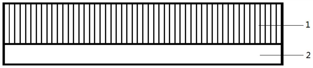
[0046] Step 4, depositing a metal nickel layer 2 on the back surface of...


PUM


Abstract

The invention discloses a manufacturing method of an n-type low-resistivity 4H-SiC ohmic contact. The manufacturing method comprises the following steps: step 1, cleaning an n-type 4H heavily doped SiC substrate; step 2, depositing a metal nickel layer on the back surface of the n-type 4H heavily doped SiC substrate; and step 3, heating the metal nickel layer by using LPCVD equipment, so that the metal nickel layer permeates into the n-type 4H heavily-doped SiC substrate, and carrying out combination reaction on nickel metal in the metal nickel layer and SiC to form NixSiy and a carbon cluster layer, thereby completing ohmic contact. The ohmic contact of the SiC material is formed by using LPCVD equipment, the Ar gas flow and the vacuum pressure value in the chamber are stable and controllable in the annealing process, the nickel silicide/SiC system can be stably transited to the ohmic contact from Schottky contact in the progressive heating process, the structure defects induced in the complex silicification process are reduced, and under the lower high doping concentration, stable, effective and uniform NixSiy and carbon cluster layer silicide are formed, and the preparation process of ohmic contact is completed.

Description

technical field [0001] The invention belongs to the field of microelectronic manufacturing technology, in particular to an n-type low-resistivity 4H-SiC ohmic contact manufacturing method. Background technique [0002] As a representative of the third generation of new wide-bandgap semiconductor materials, SiC has an important position and Broad prospects. [0003] However, one major process technology limiting SiC electronics is the ohmic contact. At present, the development of the SiC chip industry is still in its infancy, the uniformity and stability of product parameters are poor, and the chip yield rate is low. The main reason for the low yield rate is the ohmic contact problem. Due to the large band gap of SiC, the height of the Schottky barrier formed by all metals fabricated on 4H-SiC is about 1eV, which is a serious challenge for forming low-resistivity ohmic contacts on SiC. [0004] Achieving low-resistance ohmic contact technology is a major pain point in the ...

Claims


Application Information

Patent Timeline
IPC IPC(8): H01L21/285C23C14/18C23C14/30C23C14/58
CPCH01L21/0485C23C14/18C23C14/30C23C14/5806C23C14/5846Y02P70/50
Inventor 何静博胡长青尚春林侯斌齐易晨
Owner XIAN MICROELECTRONICS TECH INST
Why Eureka
Try Eureka