Current tolerance type multi-layer PCB and preparation method thereof

A current withstand, adhesive layer technology, used in multilayer circuit manufacturing, printed circuit manufacturing, electrical components, etc.

Pending Publication Date: 2021-09-24
KALEX MULTI LAYER CIRCUIT BOARD (ZHONGSHAN) CO LTD
View PDF7 Cites 0 Cited by
  • Summary
  • Abstract
  • Description
  • Claims
  • Application Information

AI Technical Summary

Problems solved by technology

In the traditional processing process, the method of increasing the copper thickness is usually used to improve the current withstand performance of the PCB, but this method has great limitations, and it is difficult to meet the increasing current transmission requirements.

Method used


Image

  • Current tolerance type multi-layer PCB and preparation method thereof
  • Current tolerance type multi-layer PCB and preparation method thereof
  • Current tolerance type multi-layer PCB and preparation method thereof

Examples


preparation example Construction

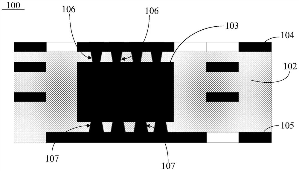
[0062] Another embodiment of the present invention provides a method for manufacturing a current-resistant multilayer PCB 100 . The preparation method comprises the steps of:

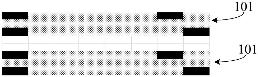
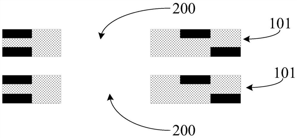
[0063] S101: Opening holes 200 on multiple inner core boards 101 and multiple prepregs to obtain through-hole core boards and through-hole prepregs respectively. For example, two inner core boards 101 are used to prepare the PCB, and the structures of the two inner core boards 101 are as follows: figure 2 As shown, after the through hole 200 is opened, a through-hole core board is obtained, and the structure of the through-hole core board is as follows image 3 shown.

[0064] S102 : Stack the through-hole core boards and the through-hole prepregs so that the through-hole prepregs are arranged between adjacent through-hole core boards, and the respective through holes 200 are connected to obtain a pre-arrangement board.

[0065] S103: Put the conductive medium 103 into the connected through holes 20...

Embodiment 1

[0091] The preparation method of PCB in the present embodiment is:

[0092] S201: Take two copper-clad laminates with a copper thickness of 3 oz, cut the inner core board as required, and make the inner layer graphics. The steps of making the inner layer graphics are grinding, rolling, exposure and development in sequence. The roll film process uses 1.5mil dry film, and the exposure process uses negative film. After the inner layer graphics are made, the inner layer circuit is inspected by graphic inspection (AOI optical inspection) to check whether the inner layer graphic circuit has open circuit, short circuit, erosion and other problems.

[0093] S202: Carry out browning treatment on the inner layer core boards that pass the pattern inspection. The steps of browning treatment are: board loading, degreasing, water washing, presoaking, browning, water washing, board drying, cooling, and board removal in sequence.

[0094] S203: Open holes for multiple prepregs: take two 30...


PUM

PropertyMeasurementUnit
frequencyaaaaaaaaaa
sizeaaaaaaaaaa
pore sizeaaaaaaaaaa

Abstract

The invention relates to a current tolerance type multi-layer PCB and a preparation method thereof. According to the preparation method, a plurality of inner-layer core plates and a plurality of prepregs are respectively subjected to through hole treatment, and then the through hole core plates and the through hole prepregs are stacked and arranged, so that through holes of the through hole core plates are communicated with through holes of the through hole prepregs. Then a conducting medium is placed into the communicated through holes, and first lamination treatment is performed to obtain a first laminated plate; and copper deposition and electroplating are performed on the first laminated plate to connect the conductive medium with the pre-arranged plate, secondary outer layer pattern processing is performed, secondary laminating treatment is performed, and the first copper foil and the second copper foil of the second laminated plate are respectively connected with the conductive medium through the first blind hole and the second blind hole. And then copper deposition treatment is carried out on the blind hole plate, and metal copper is attached to the hole walls of the first blind hole and the second blind hole. Through the preparation method, the current tolerance performance can be effectively improved.

Description

technical field [0001] The invention relates to the field of PCB processing, in particular to a current-tolerant multilayer PCB and a preparation method thereof. Background technique [0002] As one of the important components of electronic products, PCB plays a role in current conduction and signal transmission. With the continuous upgrading of electronic products, the power of the products continues to increase, and the current that needs to be transmitted is also increasing. At this time, the PCB needs to have good current tolerance performance. In the traditional processing process, the method of increasing the copper thickness is usually used to improve the current withstand performance of the PCB, but this method has relatively large limitations, and it is difficult to well meet the increasing current transmission requirements. Contents of the invention [0003] Based on this, it is necessary to provide a multilayer PCB capable of effectively improving the current w...

Claims


Application Information

Patent Timeline
Patent Type & Authority Applications(China)
IPC IPC(8): H05K3/46H05K3/40
CPCH05K3/46H05K3/4038
Inventor 李鸿辉曹振兴
Owner KALEX MULTI LAYER CIRCUIT BOARD (ZHONGSHAN) CO LTD
Why Eureka
Try Eureka