Implementation circuit and chip for TCK or ADC

A circuit and chip technology, applied in the field of digital-analog hybrid circuit control, can solve the problems of high power consumption, low integration, waste of area, etc., and achieve the effect of high speed and high integration rate

Pending Publication Date: 2021-10-08
SUZHOU POWERLINK MICROELECTRONICS
View PDF7 Cites 1 Cited by
  • Summary
  • Abstract
  • Description
  • Claims
  • Application Information

AI Technical Summary

Problems solved by technology

Existing circuits cannot be integrated into SoC or MCU systems, and the touch key detection circuits in the prior art are often wasteful in area, low in integration, high in power consumption, and difficult to meet the portability requirements of hardware implementation

Method used


Image

  • Implementation circuit and chip for TCK or ADC
  • Implementation circuit and chip for TCK or ADC
  • Implementation circuit and chip for TCK or ADC

Examples


Embodiment 1

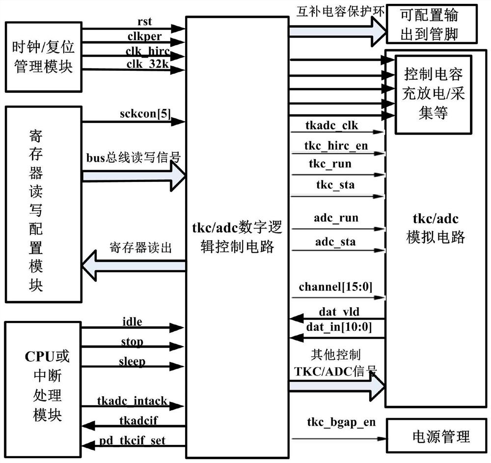
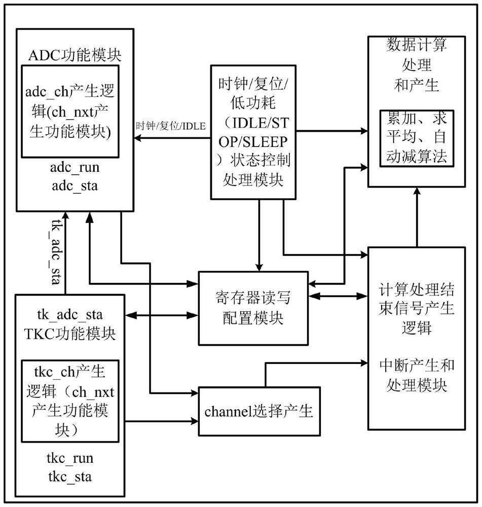
[0051] This embodiment provides an implementation circuit for TCK or ADC, which is set in SoC or MCU system, including: clock / reset / low power consumption state control processing, register read and write configuration, ADC function control module, TKC function control module , channel selection generation, data calculation processing and generation, calculation end signal and interrupt generation and processing modules.

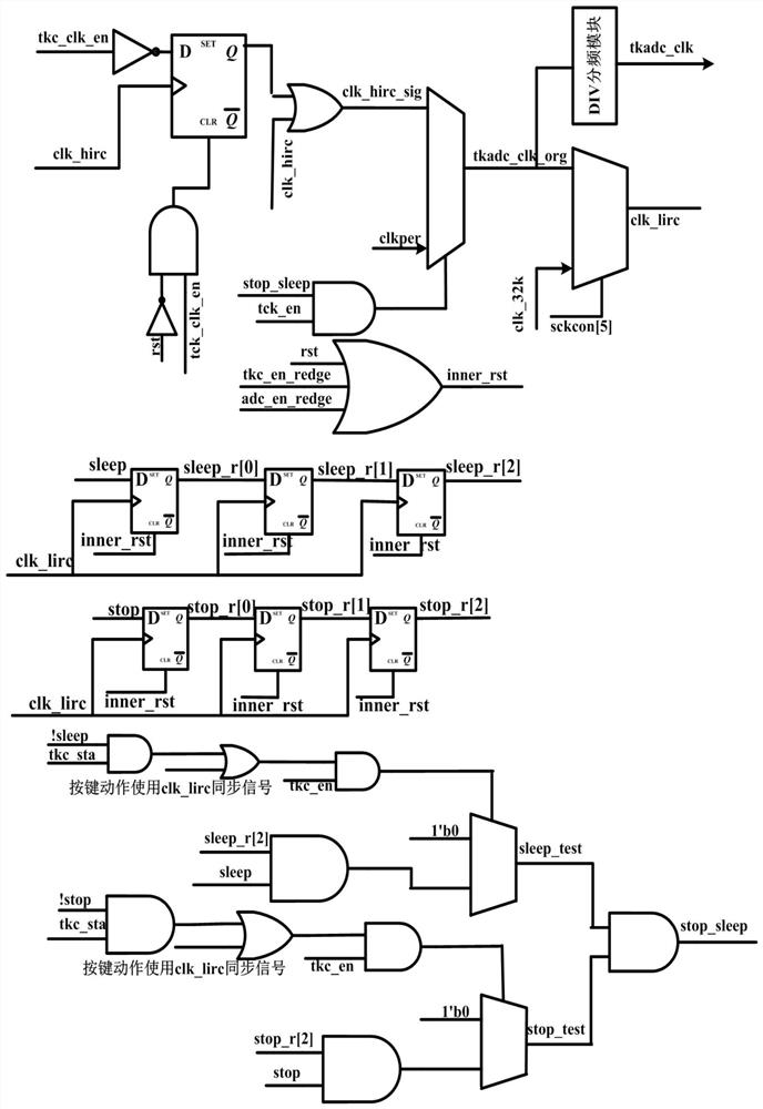
[0052] The clock / reset / low power state control processing module mainly generates internal touch key control and ADC data conversion control, clock for calculation algorithm, reset signal, and low power consumption signal (IDLE / STOP / SLEEP) is an internal low-power operation control signal generated after corresponding internal clock synchronization processing.

[0053] The register reading and writing configuration module mainly controls the TKC / ADC button channel configuration, data calculation method mode (such as accumulation, automatic polling, averaging...

Embodiment 2

[0069] This embodiment provides a system chip, wherein the internal influence or control module to complete the TKC or ADC function includes: digital logic circuit, analog implementation circuit, clock management module, chip register read and write configuration module, CPU and interrupt processing, power supply management module;

[0070] The digital logic circuit realizes wake-up through the power management module, generates the working clock inside the IP through the three-way clock provided by the clock management module and the internal logic, and is used to make the whole system choose to enter different working modes, and the working modes include: idle mode, stop mode, sleep mode and normal mode; the three clocks include a first clock, a second clock, and a third clock;

[0071] The analog implementation circuit is used to collect the charging capacitor signal (which is an analog signal) or the ADC generated by the key action of the pin when the pin function characte...


PUM


Abstract

The invention discloses an implementation circuit and a chip for a TCK or an ADC in the field of integrated circuits and semiconductors, and aims to solve the technical problems of data conversion of touch keys integrated in an SoC/MCU system, data calculation operation realized by internal hardware, analog-to-digital conversion of the ADC and data calculation. The circuit comprises modules which are integrated in an SoC/MCU system and are used for realizing corresponding functions, wherein the modules mainly comprise a digital logic circuit, an analog realization circuit, a clock management module, a register read-write configuration module, a CPU and a power supply management module. According to the invention, when the SoC/MCU chip pin is configured with a touch key function pin or an ADC data conversion function, key identification, conversion of analog signal data and data calculation can be realized through CPU operation of an SoC/MCU system and a designed hardware IP circuit.

Description

technical field [0001] The invention relates to a realization circuit and chip for TCK or ADC, and belongs to the technical field of digital-analog hybrid circuit control. Background technique [0002] With the development of integrated circuit low power consumption and highly integrated technology, there are circuits that can realize functions such as touch key detection and related control functions (TOUCHKEY referred to as TKC), digital-to-analog conversion (ADC) control and data calculation. The mechanical key has many advantages, such as: the number of keys is almost unlimited, the key will not fail due to mechanical wear, the appearance is beautiful, the cost is low, waterproof and dustproof, etc., so the capacitive touch key system is widely used in consumer electronics, objects, etc. Networking, home appliances and other occasions. The basic principle of the touch button is to detect the extra capacitance generated by the touch of a human finger, and this extra capa...

Claims


Application Information

Patent Timeline
Patent Type & Authority Applications(China)
IPC IPC(8): H03M11/20H03K17/96H03M1/12
CPCH03M11/20H03K17/96H03M1/12
Inventor 张跃玲万海军
Owner SUZHOU POWERLINK MICROELECTRONICS
Why Eureka
Try Eureka