Epitaxial wafer of AlGaN-based deep ultraviolet light emitting diode and preparation method thereof

A technology of light-emitting diodes and epitaxial wafers, which is applied to semiconductor devices, electrical components, circuits, etc., can solve the problems of affecting the quality of p-type layer crystals, high difficulty of doping, and reducing electrical conductivity, etc., so as to improve hole mobility, Increased conductivity and increased efficiency

Active Publication Date: 2021-10-29
HC SEMITEK ZHEJIANG CO LTD
View PDF3 Cites 1 Cited by
  • Summary
  • Abstract
  • Description
  • Claims
  • Application Information

AI Technical Summary

Problems solved by technology

[0004] Due to the high difficulty of doping in the p-type AlGaN layer, in order to increase the carrier concentration of the p-type layer of the AlGaN-based deep ultraviolet light-emitting diode and improve the conductivity of the p-type layer, it is usually grown on the p-type AlGaN layer The p-type GaN layer with higher carrier concentration, however, directly grows the p-type GaN layer on the p-type AlGaN layer, which is prone to the problem of lattice mismatch, resulting in more dislocation defects, which affects the p-type layer. crystal quality, which reduces conductivity

Method used


Image

  • Epitaxial wafer of AlGaN-based deep ultraviolet light emitting diode and preparation method thereof
  • Epitaxial wafer of AlGaN-based deep ultraviolet light emitting diode and preparation method thereof
  • Epitaxial wafer of AlGaN-based deep ultraviolet light emitting diode and preparation method thereof

Examples


Embodiment Construction

[0036] In order to make the purpose, technical solution and advantages of the present disclosure clearer, the implementation manners of the present disclosure will be further described in detail below in conjunction with the accompanying drawings.

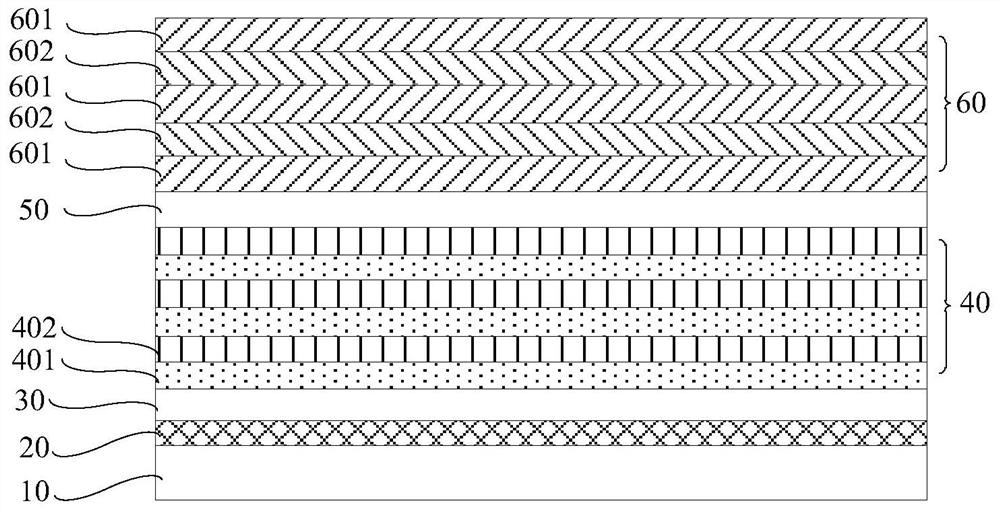
[0037] figure 1 It is a schematic structural diagram of an epitaxial wafer of an AlGaN-based deep ultraviolet light-emitting diode provided by an embodiment of the present disclosure. Such as figure 1 As shown, the epitaxial wafer includes a substrate 10 and an AlN layer 20 , an n-type AlGaN layer 30 , a multi-quantum well layer 40 , a p-type AlGaN layer 50 and a p-type ohmic contact layer 60 sequentially formed on the substrate 10 .

[0038] Wherein, the p-type ohmic contact layer 60 includes a plurality of P-type GaN layers 601 and a plurality of hexagonal boron nitride layers 602 stacked alternately in sequence, and along the direction of epitaxial wafer growth, the doping concentration of each P-type GaN layer 601 increases la...


PUM

PropertyMeasurementUnit
thicknessaaaaaaaaaa
thicknessaaaaaaaaaa
thicknessaaaaaaaaaa

Abstract

The invention provides an epitaxial wafer of an AlGaN-based deep ultraviolet light emitting diode and a preparation method of the epitaxial wafer, and belongs to the technical field of photoelectron manufacturing. The epitaxial wafer comprises a substrate, and an AlN layer, an n-type AlGaN layer, a multi-quantum well layer, a p-type AlGaN layer and a p-type ohmic contact layer which are sequentially formed on the substrate; the p-type ohmic contact layer comprises a plurality of p-type GaN layers and a plurality of hexagonal boron nitride layers which are sequentially and alternately stacked, and the doping concentration of each p-type GaN layer is increased layer by layer along the growth direction of the epitaxial wafer. According to the embodiment of the invention, the conductivity of the p-type layer can be improved, and the problem of lattice mismatching between the AlGaN layer and the p-type GaN layer is relieved, so that the crystal quality of the p-type layer is improved.

Description

technical field [0001] The disclosure relates to the technical field of optoelectronic manufacturing, in particular to an epitaxial wafer of an AlGaN-based deep ultraviolet light-emitting diode and a preparation method thereof. Background technique [0002] Light Emitting Diode (English: Light Emitting Diode, referred to as: LED), as a very influential new product in the optoelectronics industry, has the characteristics of small size, long service life, colorful colors, and low energy consumption. It is widely used in lighting, display screens , signal lights, backlight, toys and other fields. The core structure of the LED is the epitaxial wafer, and the production of the epitaxial wafer has a great influence on the photoelectric characteristics of the LED. [0003] Epitaxial wafers generally include n-type layers, multiple quantum well layers, and p-type layers. The AlGaN-based deep-ultraviolet light-emitting diode is a light-emitting diode with an emission wavelength of ...

Claims


Application Information

Patent Timeline
Patent Type & Authority Applications(China)
IPC IPC(8): H01L33/14H01L33/32H01L33/06H01L33/00
CPCH01L33/14H01L33/06H01L33/325H01L33/0066H01L33/0075
Inventor 丁涛龚程成尹涌梅劲
Owner HC SEMITEK ZHEJIANG CO LTD
Why Eureka
Try Eureka