
Processing method for processing rectangular photovoltaic cell silicon wafer by using primary single crystal silicon rod

A technology for silicon wafers and monocrystalline silicon rods for photovoltaic cells, which is applied in stone processing equipment, manufacturing tools, fine working devices, etc. Processing time and other issues, to achieve the effect of small loss, high production efficiency, and increase processing time

Active Publication Date: 2021-11-05
云南宇泽半导体有限公司
View PDF29 Cites 3 Cited by
  • Summary
  • Abstract
  • Description
  • Claims
  • Application Information

AI Technical Summary

Problems solved by technology

[0012]Second, because the truncated length of the invention CN 108068221 B silicon rod depends on the size of the opposite side of the silicon chip, the size of the opposite side of the silicon chip is small, so the monocrystalline silicon rod Shorter length, more joints during slicing, more loss of the first and last piece, more processing steps, and more auxiliary man-hours, which affect the slicing rate and production efficiency
[0013] Third, the invention CN 108068221 B needs to process the cylindrical surface of the monocrystalline silicon rod before slitting, so that part of the monocrystalline silicon that can be directly recycled becomes chips Silica fume discharge wastes material, increases emissions and increases processing time

Method used


Image

  • Processing method for processing rectangular photovoltaic cell silicon wafer by using primary single crystal silicon rod
  • Processing method for processing rectangular photovoltaic cell silicon wafer by using primary single crystal silicon rod
  • Processing method for processing rectangular photovoltaic cell silicon wafer by using primary single crystal silicon rod

Examples


Embodiment 1

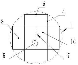
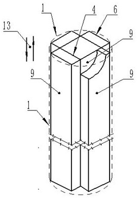
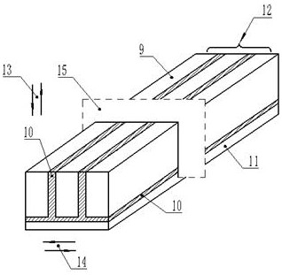
[0083] Reference attached figure 1 , attached figure 2 , attached image 3 , a processing method for processing rectangular photovoltaic cell silicon wafers with primary single crystal silicon rods, taking the processing of 162mm×54mm rectangular silicon wafers as an example, without considering the processing deviation and margin, including the following steps:

[0084] Prepare materials:

[0085] Cutting off the shoulder and the end of the primary monocrystalline silicon rod 1, and truncating the primary monocrystalline silicon rod 1 according to the maximum processing length of the slicing equipment;

[0086] Step (1), determine the vertical tangent line:

[0087] See attached figure 1 , attached figure 2 , draw four straight lines on the cross-sectional plane of the primary single crystal silicon rod 1, and the arrangement of the four straight lines on the plane is a well-shaped line, which is called a well-shaped straight line 4, and the distance between any two pa...

Embodiment 2

[0097] Reference attached figure 1 , attached figure 2 , attached Figure 4 , a processing method for processing rectangular photovoltaic cell silicon wafers with primary single crystal silicon rods, taking the simultaneous processing of two commonly used rectangular silicon wafers of 210mm×105mm and 210mm×210mm as an example, without considering the processing deviation and margin, including the following steps:

[0098] Prepare materials:

[0099] Cutting off the shoulder and the end of the primary monocrystalline silicon rod 1, and truncating the primary monocrystalline silicon rod 1 according to the maximum processing length of the slicing equipment;

[0100] Step (1), determine the vertical tangent line:

[0101] See attached figure 1 , attached figure 2 , make four well-shaped straight lines 4 on the cross-sectional plane of the primary single crystal silicon rod 1, the distance between any two parallel well-shaped straight lines 4 is 210mm, and the central rectan...

Embodiment 3

[0109] Reference attached figure 1 , attached figure 2 , attached Figure 5 , a processing method for processing rectangular photovoltaic cell silicon wafers with primary single crystal silicon rods, taking the processing of 210mm×70mm silicon wafers as an example, without considering the processing deviation and margin, including the following steps:

[0110] Prepare materials:

[0111] Cutting off the shoulder and the end of the primary monocrystalline silicon rod 1, and truncating the primary monocrystalline silicon rod 1 according to the maximum processing length of the slicing equipment;

[0112] Step (1), determine the vertical tangent line:

[0113] See attached figure 1 , attached figure 2 , make four well-shaped straight lines 4 on the cross-sectional plane of the primary single crystal silicon rod 1, the distance between any two parallel well-shaped straight lines 4 is 210mm, and the central rectangle 5 surrounded by the well-shaped straight lines 4 is 210mm×210...


PUM

PropertyMeasurementUnit
widthaaaaaaaaaa

Abstract

The invention discloses a processing method for processing a rectangular photovoltaic cell silicon wafer by using a primary single crystal silicon rod. The method comprises the following steps of step 1, determining eight longitudinal tangent lines formed by four straight lines shaped like a Chinese character "jing" and four edge straight lines on a cross section plane of the primary single crystal silicon rod; step 2, longitudinally cutting the primary single crystal silicon rod to obtain rectangular silicon ingots; step 3, splicing the rectangular silicon ingots to obtain a spliced silicon ingot; and step 4, cutting the spliced silicon ingot by using multiple planes to obtain the silicon wafer of a single crystal silicon photovoltaic cell. Compared with the prior art, the processing method is favorable for using a large-diameter single crystal silicon rod, is favorable for improving the distribution uniformity and symmetry of impurities doped in the silicon wafer, is favorable for improving the working production efficiency, and is favorable for reducing the head and tail slice loss; and in the slicing process, cutting silicon powder can be discharged, the cutting environment is improved, the production efficiency is improved, and the product quality is improved.

Description

technical field [0001] The invention relates to the technical field of monocrystalline silicon photovoltaic cells, in particular to a processing method for processing rectangular photovoltaic cell silicon wafers with raw monocrystalline silicon rods. Background technique [0002] Photovoltaic cells made of monocrystalline silicon have the advantages of mature manufacturing process, stable quality, and high photoelectric conversion efficiency. Therefore, most of the current industrialized high-efficiency silicon photovoltaic cells use monocrystalline silicon wafers as the basic material. [0003] In order to improve the packaging efficiency of photovoltaic modules, it is hoped that the monocrystalline silicon wafer has a standard, rectangular shape with no corners. In order to improve production efficiency and reduce costs, it tends to use larger area monocrystalline silicon wafers and draw larger diameter single crystals. silicon crystals. [0004] Background technology, I...

Claims


Application Information

Patent Timeline
Patent Type & Authority Applications(China)
IPC IPC(8): B28D5/00B28D5/04
CPCB28D5/045B28D5/0058B28D5/0076Y02P70/50
Inventor 王培业
Owner 云南宇泽半导体有限公司
Learn More