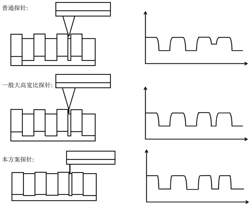
Preparation method of tip of inclined AFM probe with controllable size and inclination angle and ultra-large height-width ratio
A technology of probe tip and inclination angle, which is applied in the field of ultra-large aspect ratio tilted AFM probe tip preparation, can solve the problems of high cost and poor consistency, and achieve the effect of simple method, controllable consistency and high detection accuracy
- Summary
- Abstract
- Description
- Claims
- Application Information
AI Technical Summary
Problems solved by technology
Method used
Image
Examples
Embodiment 1
[0031] A method for preparing a tilted AFM probe tip with a controllable size and tilt angle, comprising the following steps:
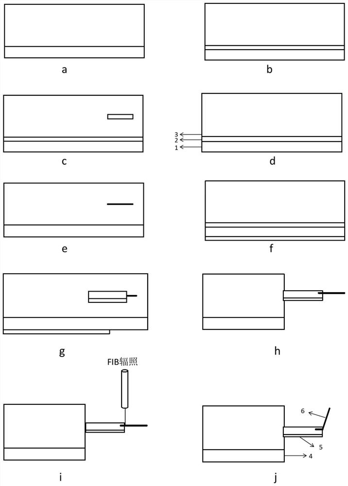
[0032] 1. Double-sided polished SOI wafers are selected as raw materials, which are composed of a device silicon layer, a silicon dioxide layer, and a substrate silicon layer, and the thicknesses are 2.5 microns, 0.5 microns and 350 microns respectively. (Such as figure 2 as shown in a)
[0033] 2. The RCA standard process cleans the sample, so that the surface of the ultraviolet lamp microscope inspection is clean and free of impurities.
[0034] 3. Spin-coat a layer of PMMA photoresist with a thickness of 200 nanometers on the surface of the sample with a forward rotation speed of 500r / min for 5s and a rear rotation speed of 4000r / min for 40s. Place it on a hot plate, heat and bake at 180°C for 1min. (Such as figure 2 b)
[0035] 4. Use an electron beam to photoresist, use an accelerating voltage of 100KeV, a beam current of 100pA, and a dose...
Embodiment 2
[0051] A method for preparing a tilted AFM probe tip with a controllable size and tilt angle, comprising the following steps:
[0052] 1. After cleaning the SOI sheet, spin-coat 200-400nm PMMA photoresist on the surface, and bake at 180°C for 1-2 minutes. The SOI wafer is composed of a device Si layer, an insulating SiO2 layer and a substrate Si layer. The thicknesses of the Si layer of the device, the SiO2 layer and the Si layer of the substrate are 1-5 microns, 0.5-2 microns and 350-500 microns respectively.
[0053] 2. Expose the spin-coated sample with an electron beam exposure machine, and the exposure dose is 500-1000 mJ / cm 2 . After the exposure is completed, put the sample into the developer for 30-50 seconds, and then put it into the fixer for 30-50 seconds.
[0054] 3. Use thermal evaporation, electron beam evaporation or magnetron sputtering equipment to directly deposit 20-30 nanometer Cr or Ti metal film. Or first deposit 3-5 nanometers of Cr or Ti adhesion la...
PUM
| Property | Measurement | Unit |
|---|---|---|
| thickness | aaaaa | aaaaa |
| length | aaaaa | aaaaa |
Abstract
Description
Claims
Application Information


