Ostwald nanometer welding method
A welding film, metal nanoparticle technology, applied in welding equipment, manufacturing tools, metal processing equipment, etc., can solve the problem of slow Ostwald ripening, limited application of Ostwald ripening, and insufficient welding mechanism. Interpretation and other issues, to achieve the effect of strong adjustability, more electrochemical active sites, and controllable speed
- Summary
- Abstract
- Description
- Claims
- Application Information
AI Technical Summary
Problems solved by technology
Method used
Image
Examples
Embodiment 1
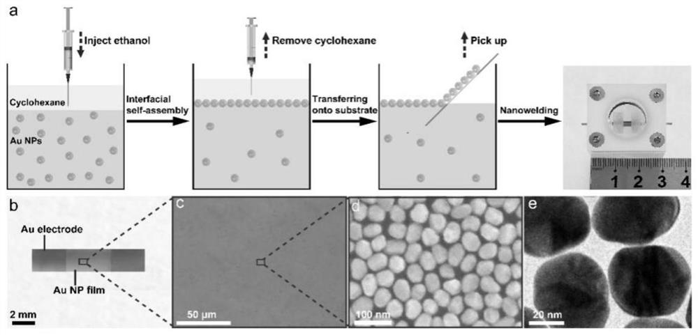
[0057] The interface self-assembly and transfer of AuNP is carried out according to the following method:
[0058] Step 1: Put 20mL of the prepared AuNP dispersion into a 50mL beaker, and then add about 5mL of cyclohexane to form a clear water-oil interface.
[0059] Step 2: Quickly inject 5 mL of ethanol to induce AuNPs to self-assemble into a dense AuNP film at the water-oil interface, then remove the cyclohexane on the upper layer of the AuNP film on the water-oil interface, and transfer the AuNP film to the corresponding substrate, Let dry naturally.
[0060] The interface self-assembly and transfer of AuNP in Example 1, and the schematic diagram of its nano-welding in the self-made nano-welding device, as well as the morphology characterization of the assembled AuNP film, please refer to figure 1 .
[0061] The AuNP thin films described in the following cases are all prepared by the method of this case unless otherwise stated.
Embodiment 2
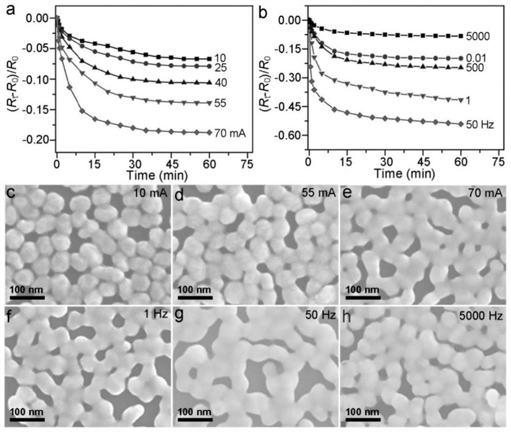
[0063] According to the following method, direct current enhanced Ostwald nano-welding of AuNP film under different current intensities is carried out:
[0064] Step 1: Use the precision test power supply B2912A to set the corresponding parameters under the conditions of outputting each current intensity.
[0065] Step 2: Place the AuNP film transferred on the glass substrate into the welding device, and weld the AuNP film under the conditions of the current intensity of 10, 25, 40, 55, and 70mA in a pure water atmosphere 0-60min, and real-time monitoring of the resistance change of the AuNP film during the welding process.
[0066] Step 3: According to the law of resistance change with time, the AuNP film after soldering under various conditions is selectively selected for morphology characterization.
[0067] In Example 2, during the strengthened Ostwald nano-welding process under different current intensities, the relative resistance change rate of the AuNP film under diff...
Embodiment 3
[0069] AC-enhanced Ostwald nano-welding of AuNP films under different AC pulse frequencies was carried out as follows:
[0070] Step 1: Fix the current intensity to 70mA, and set different AC pulse frequencies.
[0071] Step 2: Place the AuNP film transferred on the glass substrate into a welding device, and in a pure water atmosphere, and under the condition of AC pulse frequency of 0.01, 1, 50, 500, and 5000 Hz, conduct the AuNP film Welding for 0-60min, and real-time monitoring of the resistance change of the AuNP film during the welding process.
[0072] Step 3: According to the law of resistance change with time, the AuNP film after soldering under various conditions is selectively selected for morphology characterization.
[0073] In Example 3, during the alternating current enhanced Ostwald nano-welding process under different alternating current pulse frequencies, the relative resistance change rate of the AuNP film under different current intensities varies with weld...
PUM
| Property | Measurement | Unit |
|---|---|---|
| size | aaaaa | aaaaa |
Abstract
Description
Claims
Application Information
 - R&D
- Intellectual Property
- Life Sciences
- Materials
- Tech Scout
- Unparalleled Data Quality
- Higher Quality Content
- 60% Fewer Hallucinations
Browse by: Latest US Patents, China's latest patents, Technical Efficacy Thesaurus, Application Domain, Technology Topic, Popular Technical Reports.
© 2025 PatSnap. All rights reserved.Legal|Privacy policy|Modern Slavery Act Transparency Statement|Sitemap|About US| Contact US: help@patsnap.com


