High-gain photoelectric detector

A photodetector, high-gain technology, applied in circuits, electrical components, semiconductor devices, etc., can solve the problems of degraded detector response speed, limited number of photogenerated holes, high operating voltage, etc., and achieve high speed and extremely high responsivity Effects of photodetection, increased electron injection ratio, and reduced recombination loss

Pending Publication Date: 2021-11-12
SUN YAT SEN UNIV
View PDF0 Cites 0 Cited by
  • Summary
  • Abstract
  • Description
  • Claims
  • Application Information

AI Technical Summary

Problems solved by technology

[0004] However, current phototransistors and heterojunction phototransistors still have deficiencies. For example, for weak light signals or even single photon incident conditions, the number of photogenerated holes is extremely limited, and it is difficult to have a significant impact on the height of the emitter junction barrier. Limiting phototransistors to detect extremely faint light
Other common internal gain mechanisms of detectors also have their own limitations. For example, avalanche photodetectors require a low material defect density to avoid premature breakdown, and require a high operating voltage; photoconductive detectors have relatively low dark current. High, and the uncontrollable gain process that generally involves trap states will seriously degrade the response speed of the detector. Although the device can obtain high responsivity, the response speed is generally on the order of milliseconds or even seconds, and the application range is severely limited.

Method used


Image

  • High-gain photoelectric detector
  • High-gain photoelectric detector
  • High-gain photoelectric detector

Examples


Embodiment 1

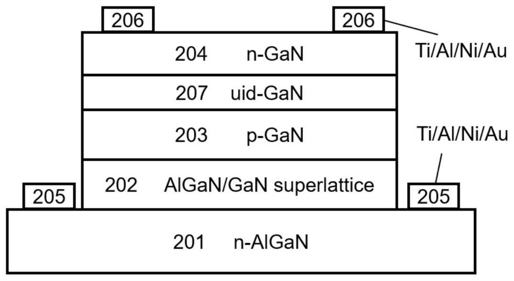
[0050] Such as figure 1 As shown, a GaN-based high-gain photodetector structure mainly includes an emitter layer 201 , a periodic quantum structure layer 202 , a base layer 203 , an absorber layer 207 and a collector layer 204 sequentially arranged from bottom to top.

[0051] In this embodiment, lower contact electrodes 205 are provided on both sides of the upper surface of the emitter layer 201 , and upper contact electrodes 206 are provided on both sides of the upper surface of the absorber layer 205 .

[0052] Wherein, the material of the emitter layer 201 is n-type AlGaN, the Al composition is 20%, and the electron concentration is 2×10 18 cm -3 , the thickness is 300nm, and the preparation method is not limited. Specifically, a substrate layer and / or a buffer layer is further provided under the emitter layer.

[0053] The periodic quantum structure layer 202 is an AlGaN / GaN superlattice structure, in which the Al component is 20%, the number of periods is 20, the thic...

Embodiment 2

[0068] The difference between this embodiment and Embodiment 1 lies in that the material of the emitter layer is n-type GaN, the periodic quantum structure layer is AlGaN (6nm) / GaN (3nm) multiple quantum wells, and the number of periods is 10.

Embodiment 3

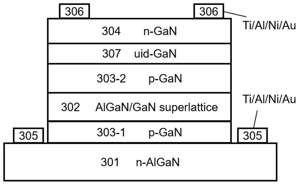
[0070] The difference between this embodiment and Embodiment 1 lies in that in the AlGaN / GaN superlattice layer of the periodic quantum structure layer, the Al composition of AlGaN is 15%, the thickness of AlGaN in each period is 3nm, and the thickness of GaN is 4nm.


PUM

PropertyMeasurementUnit
thicknessaaaaaaaaaa
thicknessaaaaaaaaaa
thicknessaaaaaaaaaa

Abstract

The invention discloses a high-gain photoelectric detector which comprises an emitting electrode, a base electrode, an absorption layer and a collector electrode which are sequentially arranged from bottom to top, and further comprises a periodic quantum structure layer which is arranged between the emitting electrode and the collector electrode or arranged in the base electrode or arranged in the emitting electrode. The periodic quantum structure layer comprises a repeated structure of a plurality of periods, and each period contains a semiconductor heterojunction. The periodic quantum structure can block diffusion of a base electrode hole to the emitting electrode and improve the electron injection ratio of an emitter junction and the amplification factor of the transistor on one hand, and on the other hand, the periodic quantum structure can bind the hole with larger effective mass in the multilayer quantum structure to reduce the recombination loss, and enables the hole life in the device to exceed the electron transport time. Therefore, a superposed photoconductive gain is generated in the phototransistor.

Description

technical field [0001] The present invention relates to the technical field of semiconductor photodetectors, more specifically, to a high-gain photodetector. Background technique [0002] Photodetectors are widely used in optical communication, imaging, environmental monitoring, assisted driving and various experimental tests. For photodetectors, responsivity is a very important index. High-responsivity semiconductor photodetectors with internal gain can realize high-sensitivity detection of weak light signals at room temperature and low bias voltage, and can save additional The signal amplifier makes the photoelectric detection system more compact, portable, and low in cost. The n-p-n type phototransistor is a commonly used semiconductor photodetector with internal gain. The principle of photoelectric gain is that when the base region is suspended, the holes generated by light absorption in the collector junction will be under the action of the built-in field and the exter...

Claims


Application Information

Patent Timeline
Patent Type & Authority Applications(China)
IPC IPC(8): H01L31/0352H01L31/11
CPCH01L31/035236H01L31/1105
Inventor 江灏吕泽升
Owner SUN YAT SEN UNIV
Why Eureka
Try Eureka