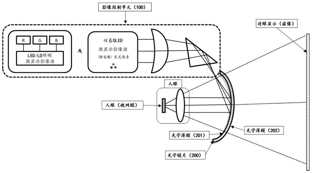
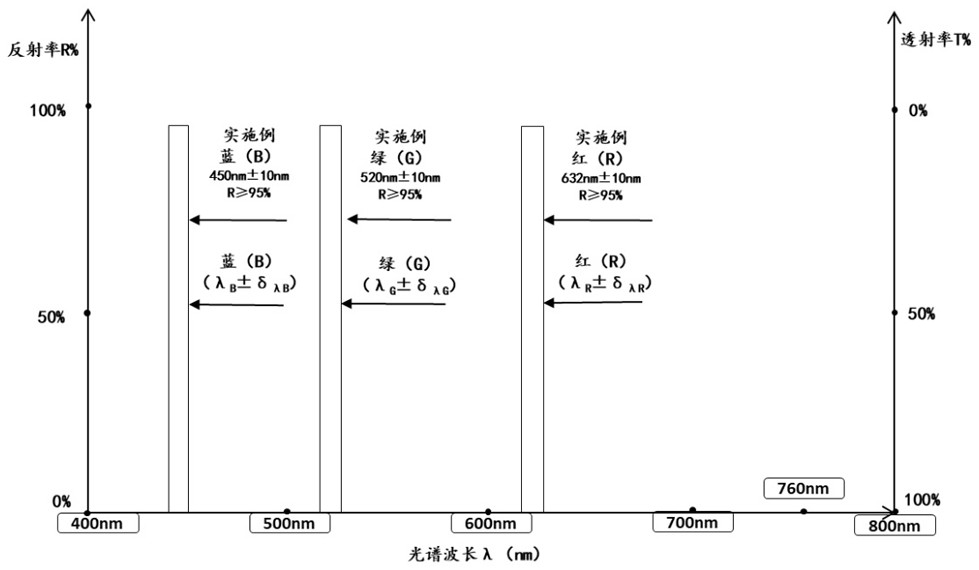
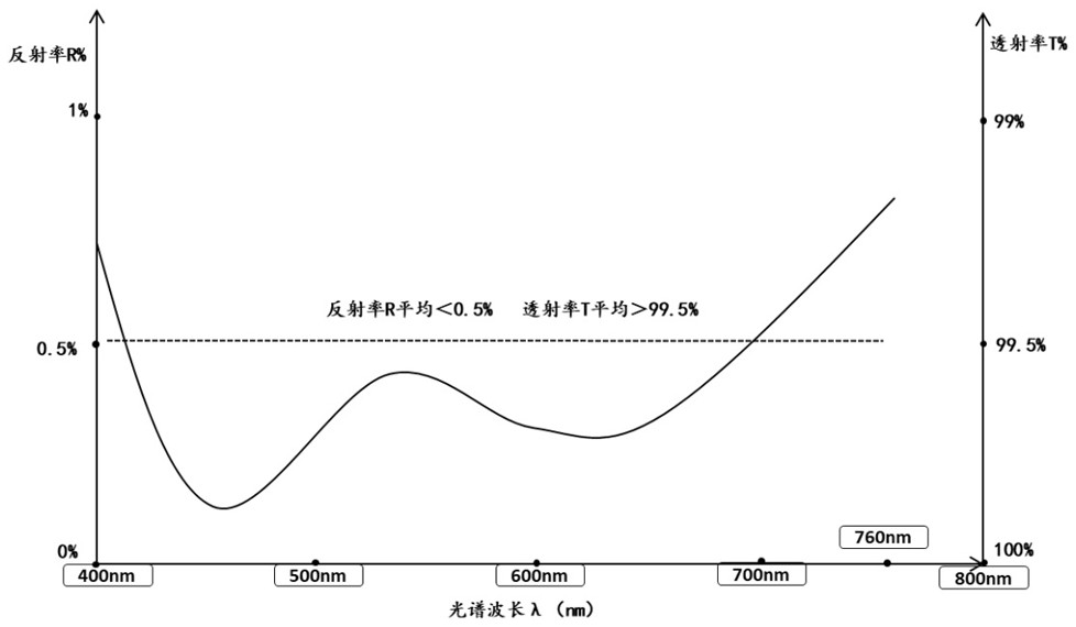
In order to achieve the best effect of near-eye display devices, people have researched and developed many structural forms of near-eye display optical systems and optical lenses, which have been applied to related products, but so far the following common problems still exist in the existing technology: imaging The structure of the display system and lens is complicated, the adaptability to the human eye is not strong, and a vision correction device is required separately, the efficiency of
light energy utilization is low, the quality of imaging display is difficult to meet the design requirements, the user experience is not good, and the
processing technology is complex and large-scale manufacturing Difficulty, high manufacturing costs, etc., have hindered the large-scale manufacturing and market promotion of related technologies and products, making it difficult for them to be quickly popularized and applied
[0004]
Early near-eye display imaging optical systems and lenses are mainly composed of multi-piece structures. Although this type of structure can achieve the effect of near-eye display, due to the relatively complex structure of the optical lens, thick optical thickness and
heavy weight, it is not compatible with the human eye. The adaptability is poor, and the physiological reactions such as dizziness and
nausea will appear when worn for a long time, and it will be gradually replaced by the new structure
In order to solve the above problems and realize the
thinning of the near-eye display system, people have researched and developed a variety of structural forms of near-eye display optical systems and lenses. According to published related patents and information reports, the new near-eye display imaging system and optical lenses are mainly Design and develop around optical
waveguide technology (including geometric optical
waveguide, diffractive optical
waveguide, holographic optical waveguide, etc.), free-form surface
prism technology, free-form surface micro-nano optical
superstructure surface technology, etc. Some of the patented technologies have been commercialized and sold. It has been pushed to the market and promoted the development and progress of near-eye display technology, but the above-mentioned existing technologies still have various deficiencies that make it difficult to meet the requirements of related
technology developmentTaking the representative optical waveguide imaging display technology as an example, the optical waveguide lens is considered to be the key development direction of the future AR near-eye display technology due to its light and thin shape structure and high light
transmittance, such as the geometric optical waveguide of Israel Lumus Arrays, "
Waveguide Components and Near-Eye Display Devices" (Application No. 201910212609.8) of China Huawei Technologies Co., Ltd., etc., diffractive optical waveguides such as the optical waveguide patent of Microsoft's HoloLens (US9372347), and the optical waveguide patent (US2018 / 0052277) published by Magic Leap ) and so on are
surface relief grating waveguides based on
lithography technology and holographic optical waveguides based on holographic technology. Their technical paths mainly revolve around planar optical waveguides to deal with the optical problems of near-eye display systems. Coupled in, and then allocated to the fan-shaped extended
exit pupil area, and finally coupled out to the human eye by the square out-
coupling area. Although the near-eye display optical system and optical lenses of the optical waveguide structure have a better
thinning effect, there are still the following shortcomings: Due to the loss of
light energy in the process of
coupling in and out of the waveguide and transmission, the
light energy utilization rate of the imaging display is low, and the
diffraction dispersion effect that is difficult to eliminate in the diffractive optical waveguide causes the image to produce "
rainbow" phenomenon and halo, and the optical waveguide lens is general It is difficult to manufacture curved lenses suitable for human eyes due to the
parallel plate structure, and the complex
processing technology of optical waveguide lenses leads to high yield and low cost. Obvious shortcomings such as
thinning,
prism dispersion effect, and poor adaptability to human eyes; the new technology of free-form surface micro-nano optical
superstructure surface, such as the patent applied by the University of Rochester (ROCHESTER) "for virtual and
augmented reality near-eye Free-form nanostructured surface of display" (
patent application number 201680028406, authorized announcement number CN107771297B, authorized announcement date 2021.04.06) mainly uses combiners, secondary mirrors, and free-form nanostructured waveguides, as stated in the claims The 28 claims are all about the supergrating structure defined by the surface of the
nanostructure, that is, cells with multiple superatoms and different aspect ratios. Its essence is to use the technical principle of reflective gratings. Lighter and thinner lenses, but the
processing technology and process involved are more complicated, and the super
grating on the surface of the
nanostructure needs to be carefully protected, otherwise the fine
nanostructure on the surface is not only easy to be scratched, but also slightly stained with
dirt will affect the imaging display Effect, technology maturity still needs time


