Manufacturing method of silicon carbide carrying disc for plasma etching and silicon carbide carrying disc

A manufacturing method and technology of silicon carbide, applied in semiconductor/solid-state device manufacturing, electrical components, circuits, etc., can solve the problems of high processing cost, long processing time, and poor understanding, so as to shorten processing time, improve processing efficiency, The effect of improving productivity

Active Publication Date: 2021-11-26
NANTONG SANZER PRECISION CERAMICS CO LTD
View PDF7 Cites 2 Cited by
  • Summary
  • Abstract
  • Description
  • Claims
  • Application Information

AI Technical Summary

Problems solved by technology

[0007] In order to solve the problem that material suppliers and processing manufacturers do not have a good understanding of materials and processing in the manufacturing process of silicon carbide carriers in the prior art, the processing time is relatively long, the processing cost is high, and no reasonable solution can be found when end users have problems. problems, and directly processing grooves on finished silicon carbide disks has the problems of high processing stress, limited groove depth, and high scrap rate. This application discloses a method for manufacturing silicon carbide carrier disks for plasma etching and silicon carbide Carrier, this manufacturing method integrates the manufacture of silicon carbide materials and the processing of the carrier structure. With the manufacture of silicon carbide materials, the carrier structure is gradually processed, which effectively improves production efficiency and greatly reduces production costs.

Method used


Image

  • Manufacturing method of silicon carbide carrying disc for plasma etching and silicon carbide carrying disc
  • Manufacturing method of silicon carbide carrying disc for plasma etching and silicon carbide carrying disc
  • Manufacturing method of silicon carbide carrying disc for plasma etching and silicon carbide carrying disc

Examples


Embodiment 1

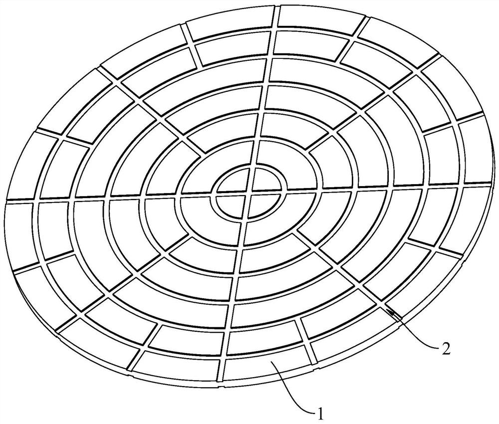
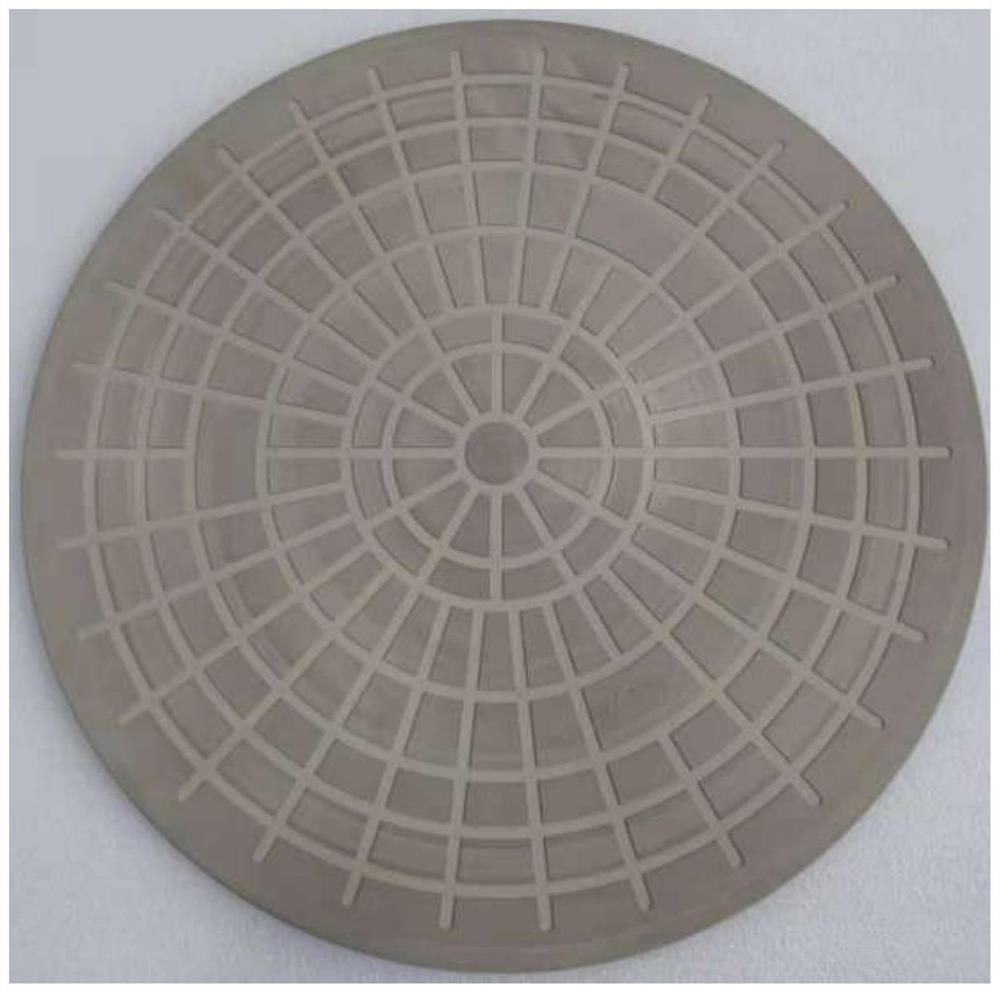
[0046] The parameters of the prepared silicon carbide carrier plate: diameter 380 mm, total thickness 4.4 mm, back groove depth 0.15 mm, back groove width 5 mm, front groove depth 1.2 mm, front groove diameter 101 mm.

[0047] The manufacturing method is as follows:

[0048] (1) Blank molding: Silicon carbide granulated powder in solid phase sintering system is used to form silicon carbide blanks that meet the size requirements through dry pressing and then isostatic pressing or direct isostatic pressing.

[0049] (2) Blank processing: According to the finished size of the plasma-etched carrier plate and the high-temperature sintering shrinkage rate, a certain sintering allowance is reserved for the outer circle, total thickness, and groove depth on the front and back sides, and the formed silicon carbide blank is processed in a machining center . After this step, the diameter of the silicon carbide blank is 464.8 mm, the total thickness is 5.8 mm, the depth of the back groov...

Embodiment 2

[0053] The parameters of the prepared silicon carbide carrier plate: diameter 380 mm, total thickness 4.4 mm, back groove depth 0.2 mm, back groove width 5 mm, front groove depth 1.2 mm, front groove diameter 102 mm.

[0054] The manufacturing method is as follows:

[0055] (1) Blank molding: Silicon carbide granulated powder in solid phase sintering system is used to form silicon carbide blanks that meet the size requirements through dry pressing and then isostatic pressing or direct isostatic pressing.

[0056] (2) Blank processing: According to the finished size of the plasma-etched carrier plate and the high-temperature sintering shrinkage rate, a certain sintering allowance is reserved for the outer circle, total thickness, and groove depth on the front and back sides, and the formed silicon carbide blank is processed in a machining center . After this step, the silicon carbide blank has a diameter of 463.8 mm, a total thickness of 5.8 mm, a reverse groove depth of 0.45 ...

Embodiment 3

[0060] The parameters of the prepared silicon carbide carrier plate: diameter 380 mm, total thickness 3.2 mm, reverse groove depth 0.15 mm, reverse groove width 5 mm, front groove depth 1 mm, front groove width 100.5 mm in diameter.

[0061] The manufacturing method is as follows:

[0062] (1) Blank molding: Silicon carbide granulated powder in solid phase sintering system is used to form silicon carbide blanks that meet the size requirements through dry pressing and then isostatic pressing or direct isostatic pressing.

[0063] (2) Blank processing: According to the finished size of the plasma-etched carrier plate and the high-temperature sintering shrinkage rate, a certain sintering allowance is reserved for the outer circle, total thickness, and groove depth on the front and back sides, and the formed silicon carbide blank is processed in a machining center . After this step, the silicon carbide blank has a diameter of 463.8 mm, a total thickness of 4.4 mm, a reverse groov...


PUM

PropertyMeasurementUnit
thicknessaaaaaaaaaa
depthaaaaaaaaaa

Abstract

The invention belongs to the technical field of carrying discs, and particularly relates to a manufacturing method of a silicon carbide carrying disc for plasma etching and the silicon carbide carrying disc. The manufacturing method of the silicon carbide carrying disc comprises the following steps of (1) forming a plain blank, namely forming the silicon carbide plain blank meeting the size requirement by adopting silicon carbide granulation powder of a solid-phase sintering system through a process of firstly performing dry pressing and then performing isostatic pressing or directly performing isostatic pressing, (2) plain blank processing: according to the finished product size and the high-temperature sintering shrinkage rate of the plasma etching carrier disc, reserving certain sintering allowance for the outer circle, the total thickness and the groove depth of the front and back surfaces, and processing the formed plain blank, (3) high-temperature sintering: carrying out high-temperature sintering on the processed silicon carbide carrier plate blank, (4) finish machining: performing precision grinding and plane grinding on the outer circle of the carrying disc, and then machining the reverse side of the carrying disc by taking the groove depth of the reverse side as a reference, processing the front surface of the carrying disc by taking the total thickness requirement of the carrying disc as a reference, and finally, precisely grinding the wafer groove until the groove depth requirement is met.

Description

technical field [0001] The application belongs to the technical field of carrier discs, and in particular relates to a method for manufacturing a silicon carbide carrier disc for plasma etching and a silicon carbide carrier disc. Background technique [0002] ICP etching (Inductively Coupled Plasma Etch), that is, inductively coupled plasma etching. The high-frequency glow discharge effect is used to activate the reactive gas into active particles, such as atoms or free radicals. These active particles diffuse to the part to be etched, react with the material to be etched, and form volatile reactants to be removed. Its advantage lies in the fast etching rate and good physical morphology can be obtained at the same time. Applied to dry etching semiconductor materials such as GaAs, GaN, InGaAs, HfOx and ZnO. [0003] ICP etching often uses a compound gas containing multiple components, the most important of which is the etching reaction gas, which chemically reacts with the ...

Claims


Application Information

Patent Timeline
Patent Type & Authority Applications(China)
IPC IPC(8): C04B35/565C04B35/622H01L21/673
CPCC04B35/565C04B35/622H01L21/673H01L21/67336C04B2235/94C04B2235/95C04B2235/6567
Inventor 闫永杰姚玉玺
Owner NANTONG SANZER PRECISION CERAMICS CO LTD
Why Eureka
Try Eureka