Single-photon avalanche photodetector and preparation method thereof

A photodetector and single-photon avalanche technology, applied in the field of optoelectronics, can solve the problems of large post-pulse, expensive, long dead time, etc., to reduce sidewall leakage current, realize avalanche amplification, and save the effect of etching process

Active Publication Date: 2021-11-26
INST OF SEMICONDUCTORS - CHINESE ACAD OF SCI
View PDF6 Cites 2 Cited by
  • Summary
  • Abstract
  • Description
  • Claims
  • Application Information

AI Technical Summary

Problems solved by technology

At present, the single photon detectors used in the communication field mainly include superconducting nanowire single photon detectors and InGaAs / InP single photon avalanche photodiodes, but superconducting nanowire single photon The photon avalanche photodiode has a large post-pulse due to carrier capture and release during the avalanche process, and it takes a relatively long dead time to release the trapped carriers, which results in a relatively long dead time and limits the single photon The working efficiency of the detector is relatively expensive, and it cannot be compatible with the process of silicon microelectronic chips, which limits the application to a certain extent

Method used


Image

  • Single-photon avalanche photodetector and preparation method thereof
  • Single-photon avalanche photodetector and preparation method thereof
  • Single-photon avalanche photodetector and preparation method thereof

Examples


Embodiment Construction

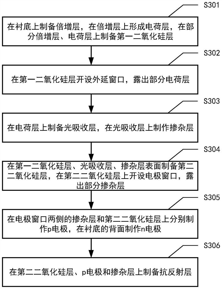
[0023] In order to make the object, technical solution and advantages of the present invention clearer, the present invention will be further described in detail below in conjunction with specific embodiments and with reference to the accompanying drawings.

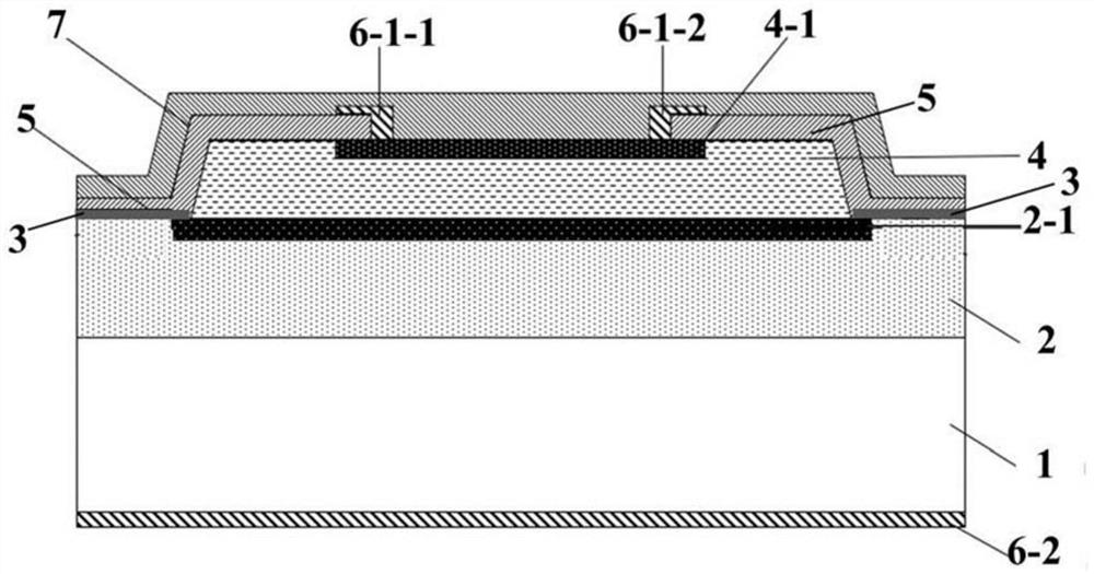
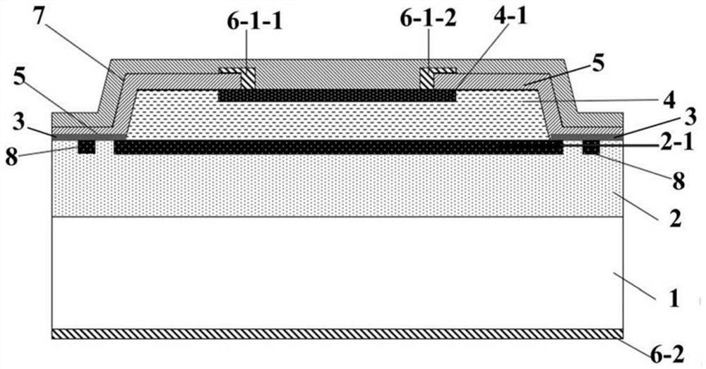
[0024] In related technologies, pure silicon single-photon avalanche photodetectors have good detection efficiency, dark count, and recovery time. However, since the band gap of silicon is 1.12eV, it cannot effectively absorb optical signals with a wavelength greater than 1100nm. , although silicon can absorb optical signals with a wavelength of less than 400nm, its penetration in silicon is very limited, so that pure silicon single photon detectors can only effectively detect optical signals of 300-1100nm, which limits its application in the communication band application. The germanium material, which is also a group four element, has high light absorption efficiency in the near-infrared band, and is fully compatible wi...


PUM

PropertyMeasurementUnit
electrical resistivityaaaaaaaaaa
thicknessaaaaaaaaaa
thicknessaaaaaaaaaa

Abstract

The invention provides a single-photon avalanche photodetector and a preparation method thereof, and the single-photon avalanche photodetector comprises a substrate; a multiplication layer which covers the substrate, wherein a charge layer is formed on the multiplication layer; a first silicon dioxide layer which covers the charge layer and part of the multiplication layer, wherein an epitaxial window is formed in the first silicon dioxide layer; a light absorption layer which is arranged in the epitaxial window, wherein a doping layer is formed on the light absorption layer; a second silicon dioxide layer which covers the surfaces of the doping layer, part of the light absorption layer and the first silicon dioxide layer, wherein an electrode window is formed in the second silicon dioxide layer, and part of the doping layer is exposed; an electrode which comprises a p electrode and an n electrode, wherein the p electrode is arranged in the electrode window, and the n electrode is arranged on the back surface of the substrate; and an anti-reflection layer which covers the second silicon dioxide layer, the p electrode and the doping layer, wherein the width of the charge layer is larger than that of the doped layer.

Description

technical field [0001] The invention relates to the field of optoelectronics, in particular to a single-photon avalanche photodetector and a preparation method thereof. Background technique [0002] Single-photon detection has broad application prospects in many fields such as quantum communication, optical time domain reflectometer, quantum key distribution (QKD), laser ranging, three-dimensional imaging, time-resolved spectroscopy, circuit testing and biological imaging, and has become an optoelectronic technology in recent years. research hotspots in the field. At present, the single photon detectors used in the communication field mainly include superconducting nanowire single photon detectors and InGaAs / InP single photon avalanche photodiodes, but superconducting nanowire single photon The photon avalanche photodiode has a large post-pulse due to carrier capture and release during the avalanche process, and it takes a relatively long dead time to release the trapped ca...

Claims


Application Information

Patent Timeline
Patent Type & Authority Applications(China)
IPC IPC(8): H01L31/107H01L31/0352H01L31/18
CPCH01L31/107H01L31/035272H01L31/18Y02P70/50
Inventor 庞雅青刘智成步文郑军薛春来
Owner INST OF SEMICONDUCTORS - CHINESE ACAD OF SCI
Why Eureka
Try Eureka