Processing method of fine micro-nano glass structure

A technology of nano glass and processing method, which is applied in the direction of microstructure technology, microstructure device, manufacturing microstructure device, etc. It can solve the problems of inability to apply glass micro-nano size structure processing, mask material compatibility, etc., to achieve processing and improve Processing efficiency, the effect of large processing

Pending Publication Date: 2021-12-14
SHANGHAI JIAO TONG UNIV
View PDF1 Cites 1 Cited by
  • Summary
  • Abstract
  • Description
  • Claims
  • Application Information

AI Technical Summary

Problems solved by technology

However, this patent has the following disadvantages: the mask material of this patent is not compatible with

Method used


Image

  • Processing method of fine micro-nano glass structure
  • Processing method of fine micro-nano glass structure
  • Processing method of fine micro-nano glass structure

Examples


Embodiment 1

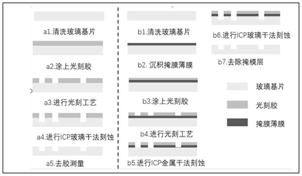
[0045] This embodiment 1 relates to a preparation method for finely processing a micro-nano glass structure, wherein the minimum size of the structure to be processed is 2 microns, and the preparation method of the micro-nano glass structure includes the following steps:

[0046]Clean the 1mm thick 4inch quartz substrate; deposit a layer of Cr film with a thickness of 130nm; then coat the photoresist on the Cr film, and make the grid structure by photolithography by ultraviolet exposure; use inductively coupled reactive ion etching Technology to etch Cr film and quartz substrate; the process parameters of etching Cr film are etching power 400W, bias RF power 40W; gas and flow rate are chlorine gas 55sccm, pressure 10mTorr. The process parameters of etching quartz substrate are etching power 1400W, bias RF power 400W; etching temperature is 58°C; gas and flow rate are Ar (auxiliary gas) 35sccm, CHF 3 110sccm, the air pressure is 45mTorr;

[0047] Use acetone ultrasonic cleani...

Embodiment 2

[0051] This embodiment 2 relates to a preparation method for finely processing the micro-nano glass structure, wherein the minimum size of the structure to be processed is 200nm, and the preparation method of the micro-nano glass structure includes the following steps:

[0052] Prepare quartz glass with a substrate thickness of 600um, and perform inorganic standard cleaning on the quartz glass to be processed; apply photoresist with a thickness of 400nm on the glass surface; transfer the processed structure to the substrate by electron beam direct writing exposure On the photoresist on the surface; use inductively coupled reactive ion etching technology to etch quartz glass, the parameters are etching power 1200W, bias RF power 200W, Ar (auxiliary gas) 35sccm, CHF 3 110sccm, the gas pressure is 35mTorr; the etching temperature is 50°C.

[0053] The photoresist is removed by ultrasonic cleaning with acetone.

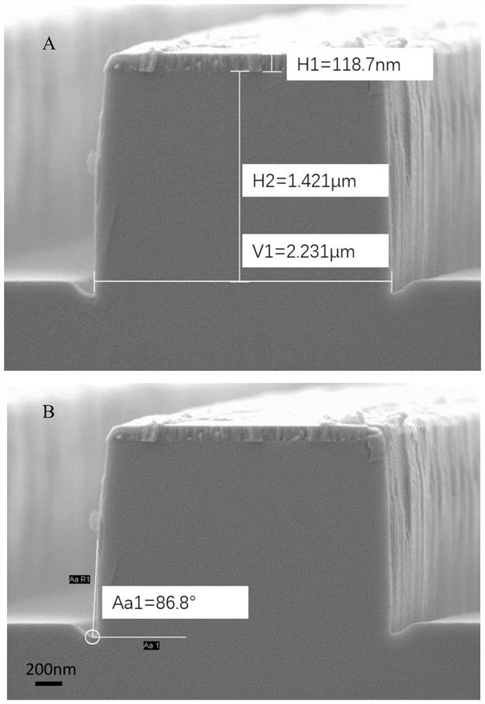
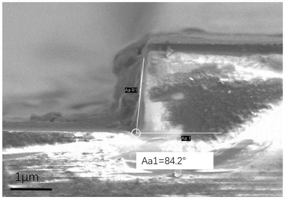
[0054] Using the preparation method of Example 2, the glass etchin...

Embodiment 3

[0056] This embodiment is basically the same as Embodiment 1, the only difference is that: the Cr film and the quartz substrate are etched by inductively coupled reactive ion etching technology; the process parameters for etching the quartz substrate are etching power 800W, bias radio frequency power 500W; the etching temperature is 60°C, the gas and flow rate for etching the quartz substrate are Ar (auxiliary gas) 35sccm, CHF 3 200 sccm, the gas pressure is 120 mTorr; the gas and flow rate for etching the Cr film are 55 sccm chlorine gas, and the gas pressure is 10 mTorr.

[0057] Using the preparation method of this example, the glass etching efficiency is 350nm / min, the etching verticality is 91°, and the roughness is <50nm.


PUM

PropertyMeasurementUnit
Thicknessaaaaaaaaaa
Etching poweraaaaaaaaaa
Roughnessaaaaaaaaaa

Abstract

The invention discloses a processing method of a fine micro-nano glass structure, which comprises the following steps: preparing a glass substrate, and cleaning and blow-drying the glass substrate; when the mask material is a non-photoresist material, depositing the mask film on the glass substrate, and then coating the photoresist; when the mask material is a photoresist material, coating photoresist on the glass substrate; transferring a structure to be processed onto the photoresist on the surface of the substrate in a photoetching manner; when the mask material is a non-photoresist material, the mask material being etched firstly, and then the glass substrate being etched; when the mask material is a photoresist material, only the glass substrate being etched; and removing the photoresist and the mask material by using a dry etching or wet etching method to form a final glass device structure. By adopting the preparation process disclosed by the invention, the glass etching rate can reach 710nm/min, the roughness is reduced to be below 40nm, and the side wall perpendicularity is close to 90 degrees.

Description

technical field [0001] The invention relates to the technical field of micro-nano glass structure preparation, and relates to a processing method for a fine micro-nano glass structure. Background technique [0002] With the development of micro-nano technology and the continuous improvement of processing technology, glass materials have excellent dielectric properties, similar thermal expansion coefficients to silicon, good thermal stability, and have some characteristics that silicon does not have, such as excellent optical properties and surface properties, etc. , is regarded as one of the ideal micro-nano processing materials, and has broad applications in the fields of optical communication, micro-electromechanical, radio frequency, micro-nanofluidic devices and three-dimensional integration. As the micro-nano structures processed on glass substrates become more and more complex, the requirements for glass processing technology are also getting higher and higher. For exa...

Claims


Application Information

Patent Timeline
IPC IPC(8): B81C1/00G03F7/00B82Y30/00B82Y40/00
CPCB81C1/00396B81C1/00531B81C1/00539G03F7/00B82Y30/00B82Y40/00
Inventor 权雪玲程秀兰刘民付学成瞿敏妮黄胜利凌天宇
Owner SHANGHAI JIAO TONG UNIV
Why Eureka
Try Eureka