Photoelectric synaptic device array, preparation method thereof and image processing equipment
A synaptic device, photoelectric technology, applied in the direction of electrical components, semiconductor devices, circuits, etc., can solve problems such as crosstalk, leakage current crosstalk, circuit leakage current crosstalk, etc., to achieve enhanced conductance, improved efficiency and power consumption, and small size Effect
- Summary
- Abstract
- Description
- Claims
- Application Information
AI Technical Summary
Problems solved by technology
Method used
Image


Examples
preparation example Construction
[0065] The present disclosure provides a method for preparing a photoelectric synapse device array, including the following steps:
[0066] S210, preparing a bottom electrode on the substrate.
[0067] Specifically, select a substrate, such as Si / SiO polished on one side 2 The substrate was first cleaned with a mixed solution of concentrated sulfuric acid and hydrogen peroxide for 30 minutes, then ultrasonically oscillated with acetone, ethanol, and deionized water at 75% power for 5 minutes, and then dried with nitrogen to clean the surface of the substrate. Clean up.
[0068] The bar-shaped bottom electrode is prepared on the cleaned substrate by photolithography, DC sputtering process and lift-off process. in:
[0069] The photolithography process specifically includes the following operations: spin-coat negative resist on the substrate (for example, 6000rpm, 20s), and then go through pre-baking (for example, 110°C, 2min), UV exposure (for example, 300W, 30s), post-bakin...
Embodiment
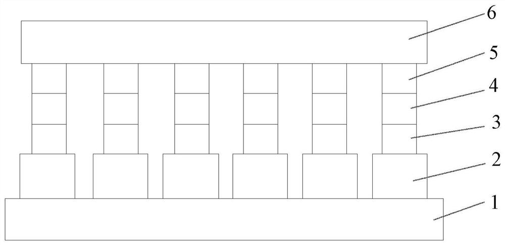
[0089] In this embodiment, using as Figure 1A and Figure 1B The shown photoelectric synapse device array structure, specifically, the photoelectric synapse device array includes a substrate 1, a bar-shaped bottom electrode 2, a P-type semiconductor layer 3 and an N-type semiconductor layer stacked on the bottom electrode 2 in sequence. 4. The light absorbing layer 5 and the transparent bar-shaped top electrode 6 . The materials of each layer are: substrate 1 is Si / SiO 2 , the horizontal rod-shaped bottom electrode 2 is Ti / Pt, and the P-type semiconductor layer 3 is NiO y , N-type semiconductor layer 4 is WO 3-z , The light absorbing layer 5 is ITO with a high degree of oxidation x The material, the bar-shaped top electrode 6 is ITO. Based on the above structure, the photoelectric synapse device array (Pt / NiO y / WO 3-z / ITO x / ITO), where each intersection forms a single optoelectronic synapse device unit (Pt / NiO y / WO 3-z / ITO x / ITO).
PUM
| Property | Measurement | Unit |
|---|---|---|
| electron work function | aaaaa | aaaaa |
| thickness | aaaaa | aaaaa |
| thickness | aaaaa | aaaaa |
Abstract
Description
Claims
Application Information