GaN-based radio frequency device with terminal structure and manufacturing method of device

A technology of radio frequency devices and terminal structures, which is applied in semiconductor/solid-state device manufacturing, semiconductor devices, electrical components, etc. It can solve the problems of weakening the frequency characteristics of devices and affecting the application scenarios of microwave devices, so as to provide frequency characteristics and gain and reduce leakage current, reducing the effect of electric field spikes

Pending Publication Date: 2021-12-17
XIDIAN UNIV
View PDF11 Cites 0 Cited by
  • Summary
  • Abstract
  • Description
  • Claims
  • Application Information

AI Technical Summary

Problems solved by technology

However, when a device with a field plate structure operates in the millimeter wave frequency band above 30 GHz, parasitic capacitance will be introduced, which will weaken the frequency characteristics of the device and affect the application scenarios of microwave devices

Method used


Image

  • GaN-based radio frequency device with terminal structure and manufacturing method of device
  • GaN-based radio frequency device with terminal structure and manufacturing method of device
  • GaN-based radio frequency device with terminal structure and manufacturing method of device

Examples


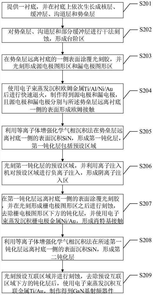
Embodiment Construction

[0042] The present invention will be described in further detail below in conjunction with specific examples, but the embodiments of the present invention are not limited thereto.

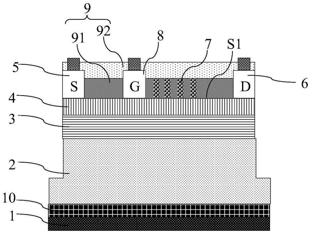
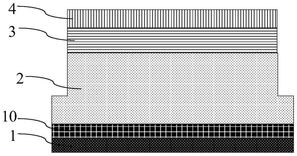
[0043] figure 1 It is a schematic structural diagram of a GaN device with a terminal structure provided by an embodiment of the present invention. See figure 1 , the present invention provides a GaN-based radio frequency device with a terminal structure, comprising: a substrate 1;

[0044] A nucleation layer 10 located on one side of the substrate 1;

[0045] The buffer layer 2 located on the side of the nucleation layer 10 away from the substrate;

[0046] The channel layer 3 located on the side of the buffer layer 2 away from the substrate 1;

[0047] The barrier layer 4 located on the side of the channel layer 3 away from the substrate 1, along the direction perpendicular to the plane where the substrate 1 is located, the barrier layer 4 includes a first surface S1 away from the channel laye...


PUM

PropertyMeasurementUnit
thicknessaaaaaaaaaa
thicknessaaaaaaaaaa

Abstract

The invention discloses a GaN-based radio frequency device with a terminal structure and a manufacturing method of the device. The radio frequency device comprises a substrate, a nucleating layer, a buffer layer, a channel layer and a barrier layer, wherein the nucleating layer, the buffer layer, the channel layer and the barrier layer are sequentially located at one side of the substrate. In the direction perpendicular to the plane where the substrate is located, the barrier layer comprises a first surface away from the channel layer, the source electrode and the drain electrode are oppositely arranged at the two sides of the first surface, and the gate electrode is located between the source electrode and the drain electrode. The passivation layer is positioned at the side, far away from the substrate, of the barrier layer and comprises a first passivation layer and a second passivation layer; the first passivation layer comprises an anion injection region, and the orthographic projection of the anion injection region is located between the gate electrode and the drain electrode in the direction perpendicular to the plane where the substrate is located, so that a negative charge center can be generated in the first passivation layer, the peak of a gate pin electric field is reduced, the breakdown voltage of the device is improved, the leakage current is reduced, and the on-state characteristic of the device is improved.

Description

technical field [0001] The invention belongs to the technical field of semiconductors, and in particular relates to a GaN-based radio frequency device with a terminal structure and a manufacturing method thereof. Background technique [0002] With the rapid development of informatization, wireless communication, radar, satellite and other fields have put forward higher requirements for microwave high-power devices, and gallium nitride materials developed in recent years are the representative of the third-generation wide-bandgap semiconductor materials. , the gallium nitride-based heterojunction forms a two-dimensional electron gas channel with high concentration and high mobility, so that the gallium nitride-based field effect transistor has a large band gap, a high critical breakdown field strength, a large thermal conductivity, and a saturated The characteristics of high electron drift speed and high carrier mobility are especially suitable for high-voltage, high-temperat...

Claims


Application Information

Patent Timeline
Patent Type & Authority Applications(China)
IPC IPC(8): H01L29/06H01L29/778H01L21/335
CPCH01L29/0653H01L29/7787H01L29/66462
Inventor 马晓华芦浩侯斌霍腾杨凌张濛鲁微郝跃
Owner XIDIAN UNIV
Why Eureka
Try Eureka