Processing method for cutting silicon wafer by utilizing time-resolved shadow imaging technology to assist laser liquid phase ablation

A shadow imaging and time-resolution technology, which is applied in stone processing equipment, laser welding equipment, metal processing equipment, etc., can solve the problems of silicon wafer surface pollution, lower production efficiency, and affect performance, so as to optimize repetition frequency and reduce defects. effect of influence

Pending Publication Date: 2022-01-11
SHANDONG UNIV OF TECH
View PDF0 Cites 0 Cited by
  • Summary
  • Abstract
  • Description
  • Claims
  • Application Information

AI Technical Summary

Problems solved by technology

However, laser ablation cutting is often accompanied by a series of defects: (1) large-scale redeposition of spatter particles generated by laser cutting, contamination of the silicon wafer surface, affecting performance; (2) melting back phenomenon of the silicon wafer surface, after cutting The originally separated parts are bonded again due to incomplete laser ablation, and a recast layer is formed on the surface, which reduces production efficiency and increases the scrap rate
Some researchers use a water jet auxiliary device to inject water into the processing area, and the water flow scours the air bubbles trapped on the surface, such as the literature "Bao J, Long Y, Tong Y, et al. Experiment and simulationst

Method used


Image

  • Processing method for cutting silicon wafer by utilizing time-resolved shadow imaging technology to assist laser liquid phase ablation
  • Processing method for cutting silicon wafer by utilizing time-resolved shadow imaging technology to assist laser liquid phase ablation
  • Processing method for cutting silicon wafer by utilizing time-resolved shadow imaging technology to assist laser liquid phase ablation

Examples


Embodiment Construction

[0044] The following will clearly and completely describe the technical solutions in the embodiments of the present invention in conjunction with the drawings in the embodiments of the present invention. Obviously, the described example is only one embodiment of the present invention, not all embodiments. Based on the embodiments of the present invention, all other embodiments obtained by persons of ordinary skill in the art without making creative efforts belong to the protection scope of the present invention.

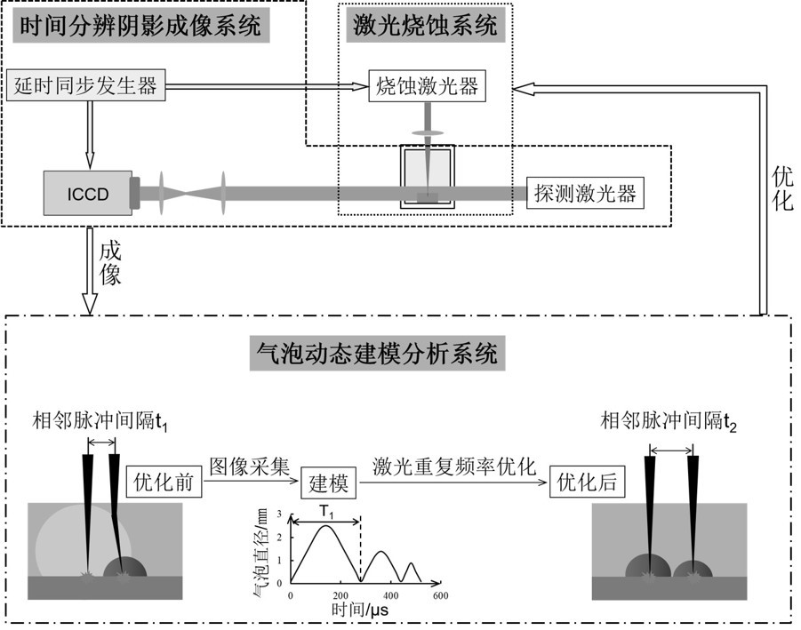
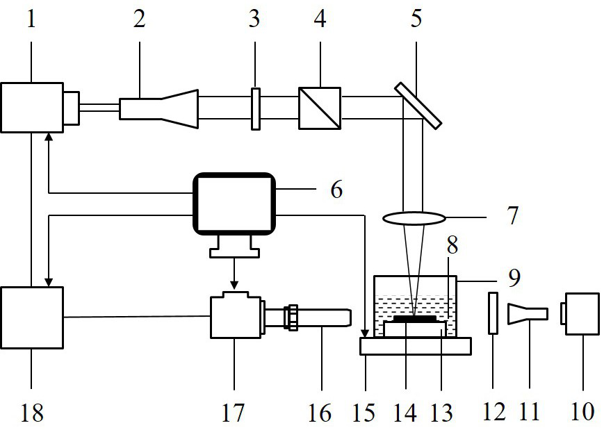
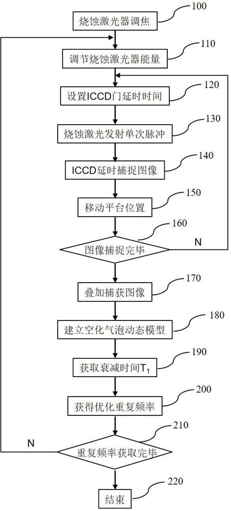
[0045] see figure 1 , figure 1 Schematic diagram of the method for optimizing liquid-assisted laser ablation cutting silicon wafer processing parameters based on time-resolved shadow imaging technology, including ablation laser system, time-resolved shadow imaging system and bubble dynamic modeling and analysis system, in which the ablation laser system burns Silicon wafers are etched to induce bubbles, the time-resolved shadow imaging system captures bubble shadow ...


PUM

PropertyMeasurementUnit
Diameteraaaaaaaaaa

Abstract

The invention discloses a processing method for cutting a silicon wafer by utilizing a time-resolved shadow imaging technology to assist laser liquid phase ablation in the technical field of laser,. Shadow images of cavitation bubbles and persistent bubbles are captured through an established time-resolved shadow imaging system, and dynamic models of the cavitation bubbles and the persistent bubbles are established; according to the dynamic model of the cavitation bubbles, the repetition frequency of the ablation laser is optimized, and the adverse effect of cavitation bubble refraction on the surface of the silicon wafer is reduced; the type and concentration of a liquid medium are optimized according to the dynamic model of the persistent bubbles, the residence time of the persistent bubbles is regulated and controlled, the persistent bubbles staying on the surface of the silicon wafer for a long time are prevented from reacting with subsequent laser pulses, and the adverse effect of the rupture impact effect of the persistent bubbles on the surface of the silicon wafer is relieved; and the processing method provided by the invention is utilized to process the silicon wafer, the obtained kerf is narrow, the heat affected zone is small, the sputter deposition range of the micro-nano particles is small, and the negative influence of induced bubbles is small.

Description

technical field [0001] The invention belongs to the field of laser processing, and is a method for optimizing processing parameters by capturing and regulating bubble dynamics, which is used for precision cutting of silicon wafers, and in particular relates to a method based on time-resolved shadow imaging. Background technique [0002] Silicon is widely used in photovoltaic cells, integrated circuit chips and other industries because of its excellent electrical and mechanical properties. Due to the heat dissipation requirements of electronic products, the thickness of a single chip is gradually reduced, and the compressive and tensile strength of thin silicon wafers is low, and it is more sensitive to external mechanical stress. Therefore, the traditional diamond cutting process is no longer suitable for scribing thickness less than 200 microns. silicon wafer. Laser cutting technology is a non-contact processing technology, and the beam after beam expansion and refocusing ...

Claims


Application Information

Patent Timeline
IPC IPC(8): B23K26/362B23K26/70B28D5/00B28D7/00
CPCB23K26/362B23K26/702B28D5/00B28D5/0064B23K2103/50B23K2103/56
Inventor 王志文田文涛王成金袁伟魏娟郑宏宇
Owner SHANDONG UNIV OF TECH
Why Eureka
Try Eureka