Crystalline silicon solar battery piece capable of inhibiting electric leakage of cutting edge, battery assembly and preparation method of crystalline silicon solar battery piece

A solar cell and cutting edge technology, applied in the field of solar cells, can solve the problems affecting the separation and collection of carriers and the loss of electrical performance of half-cell cells, and achieve the effect of avoiding the loss of electrical performance

Pending Publication Date: 2022-01-21
ZHEJIANG UNIV
View PDF2 Cites 1 Cited by
  • Summary
  • Abstract
  • Description
  • Claims
  • Application Information

AI Technical Summary

Problems solved by technology

[0005] However, for crystalline silicon solar cells with existing structures, after the cells are slit by laser scribing, a large number of recombination centers will be formed on the exposed cut sections, which will affect the separation and collection of carriers. The most important loss comes from Due to the leakage of the pn junction of the cut section, this will lead to a serious loss of electrical performance of the half-cell battery

Method used


Image

  • Crystalline silicon solar battery piece capable of inhibiting electric leakage of cutting edge, battery assembly and preparation method of crystalline silicon solar battery piece
  • Crystalline silicon solar battery piece capable of inhibiting electric leakage of cutting edge, battery assembly and preparation method of crystalline silicon solar battery piece
  • Crystalline silicon solar battery piece capable of inhibiting electric leakage of cutting edge, battery assembly and preparation method of crystalline silicon solar battery piece

Examples


Embodiment 2

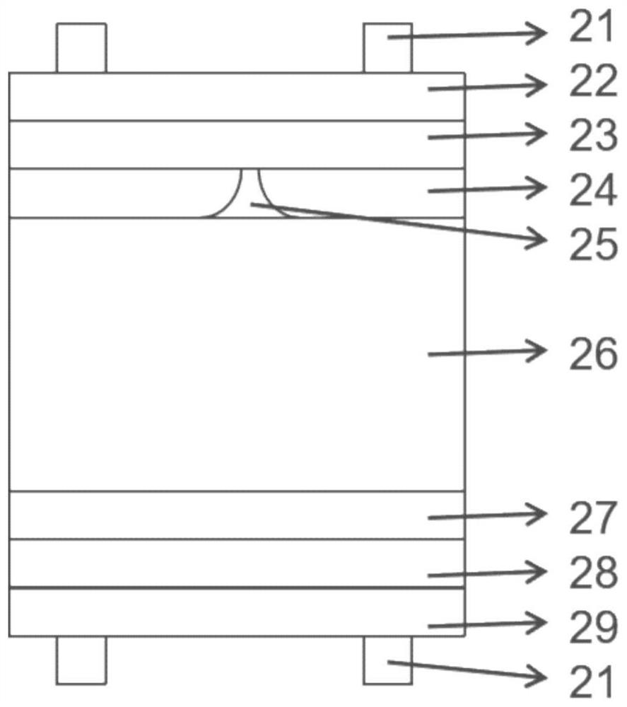
[0053] Such as figure 2 As shown, a crystalline silicon solar cell with a TOPCon structure that suppresses leakage at the cutting edge, its preparation process is as follows:

[0054] (1) Provide an n-type crystalline silicon wafer 26 for cleaning and texturing; wherein, the resistivity of the n-type crystalline silicon wafer 26 is 0.5-1.5 Ω·cm; the thickness of the n-type crystalline silicon wafer 26 is 100-160 μm.

[0055] (2) Put the obtained silicon wafer into an industrial high-temperature diffusion furnace to carry out high-temperature boron diffusion on the front to form a boron expansion layer 24, and then remove the borosilicate glass and winding plating formed during the diffusion process; wherein the boron source is boron tribromide , the boron diffusion temperature is 750-1000°C, the time is 60-180 minutes, and the square resistance value after boron diffusion is 60-120Ω / sqr.

[0056] (3) form a layer of photoresist by spin coating or spraying method on the front...

Embodiment 3

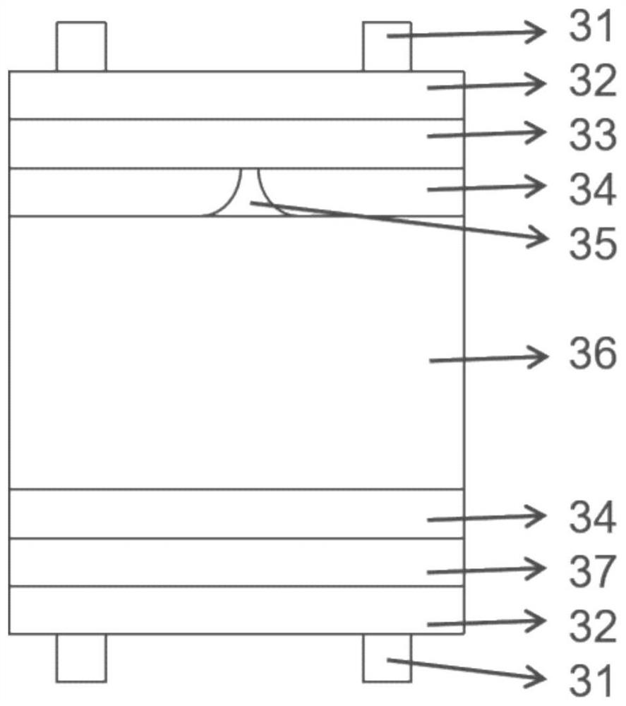
[0063] Such as image 3 As shown, a crystalline silicon solar cell with an HJT structure that suppresses leakage at the cut edge, the preparation process is as follows:

[0064] (1) Provide an n-type crystalline silicon wafer 36 for cleaning and texturing; wherein, the resistivity of the n-type crystalline silicon wafer 36 is 0.5-1.5 Ω·cm; the thickness of the n-type crystalline silicon wafer 36 is 80-140 μm.

[0065] (2) Form an intrinsic amorphous silicon layer or hydrogenated intrinsic amorphous silicon thin layer 34 on both sides of the obtained silicon wafer; wherein, the intrinsic amorphous silicon layer or hydrogenated intrinsic amorphous silicon thin layer 34 can pass through Plasma-enhanced chemical vapor deposition and other methods; the thickness of the intrinsic amorphous silicon layer or hydrogenated intrinsic amorphous silicon thin layer 34 is 1.5-4 nm.

[0066] (3) Prepare p+ type doped amorphous silicon thin layer 33 and n+ type doped amorphous silicon thin la...


PUM

PropertyMeasurementUnit
Widthaaaaaaaaaa
Thicknessaaaaaaaaaa
Resistivityaaaaaaaaaa

Abstract

The invention discloses a crystalline silicon solar battery piece capable of inhibiting electric leakage of cutting edge, a battery assembly and a preparation method of the crystalline silicon solar battery piece. In a preparation process, a cleaned and textured p-type or n-type silicon wafer is adopted; after a pn junction is formed on the front surface of the silicon wafer, a diffusion precursor layer with a doping type the same as the doping type of a silicon wafer substrate is firstly formed in an area near the center line of a silicon wafer to be subjected to laser scribing; then the doping type of an emitting electrode covered by the area is converted to be the same as the doping type of the silicon wafer substrate in manners of annealing, laser treatment, current injection or ion injection and the like; and finally, the battery piece is formed through a battery process. According to the invention, the cutting edge of an obtained half battery piece does not have a pn junction, and electrical property loss caused by the electric leakage of the pn junction at the cutting edge is avoided, so the half battery piece with higher conversion efficiency and the solar battery assembly with higher output power can be obtained.

Description

technical field [0001] The invention belongs to the field of solar cells, and in particular relates to a crystalline silicon solar battery sheet, a battery module and a preparation method for suppressing cutting edge leakage. Background technique [0002] In order to reduce the manufacturing cost of crystalline silicon solar cells, Czochralski monocrystalline silicon and cast crystalline silicon for photovoltaics are constantly developing in the direction of large size. The increase of the cell area will lead to the increase of the current, which will cause greater power loss. . However, since the current is halved after the cell is cut into half pieces, the power loss of the module can be significantly reduced, so the mainstream module technology is equipped with laser cutting equipment. [0003] For example, the Chinese patent literature with the publication number CN211957655U discloses a solar cell suitable for making half-sheet solar cells. A cross-shaped gap is arrang...

Claims


Application Information

Patent Timeline
IPC IPC(8): H01L31/0352H01L31/068H01L31/0747H01L31/18H01L31/20
CPCH01L31/0352H01L31/068H01L31/0747H01L31/1804H01L31/202Y02E10/547Y02P70/50
Inventor 余学功胡泽晨杨德仁
Owner ZHEJIANG UNIV
Why Eureka
Try Eureka