Preparation method and application of silicon-based MEMS gas sensor chip

A gas sensor and chip technology, which is applied in semiconductor/solid-state device components, instruments, scientific instruments, etc., can solve the problems of poor stability of silicon-based MEMS gas sensor chips, achieve consistent film thickness and specific surface area, and strengthen interface bonding Increased strength, improved consistency and job stability

Pending Publication Date: 2022-02-08
HUAZHONG UNIV OF SCI & TECH
View PDF0 Cites 2 Cited by
  • Summary
  • Abstract
  • Description
  • Claims
  • Application Information

AI Technical Summary

Problems solved by technology

[0004] Aiming at the above defects or improvement needs of the prior art, the present invention provides a preparation method and application of a silicon-based MEMS gas sensor chip to solve the poor stability of the silicon-based MEMS gas sensor chip prepared in the prior art question

Method used


Image

  • Preparation method and application of silicon-based MEMS gas sensor chip
  • Preparation method and application of silicon-based MEMS gas sensor chip
  • Preparation method and application of silicon-based MEMS gas sensor chip

Examples


Embodiment 1

[0046] A method for preparing a silicon-based MEMS gas sensor chip, such as figure 1 shown, including the following steps:

[0047] S1. Depositing an insulating material on the upper surface of the silicon wafer substrate to form a cantilever support layer covering the silicon wafer substrate;

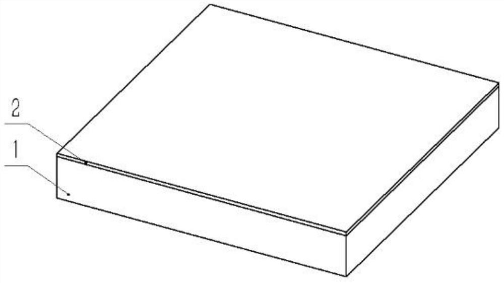
[0048] Specifically, such as figure 2 As shown, a cantilever support layer 2 is prepared on the surface of a substrate silicon wafer 1 . The insulating material can be oxide or nitride or a mixture of both, preferably an ONO composite film. In this embodiment, a silicon wafer of 4-12 inches is used as a substrate, and a support layer of silicon oxide, silicon nitride or a composite film (total thickness 300nm-2um) is prepared on the substrate by thermal oxidation growth, PECVD or LPCVD process.

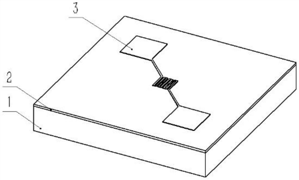
[0049] S2. Wafer-level lithography on the surface of the above-mentioned cantilever support layer and depositing metal to form a heating electrode; wherein, the material of the heating ele...

Embodiment 2

[0068] A silicon-based MEMS gas sensor chip, prepared by the method for preparing a silicon-based MEMS gas sensor chip provided in Example 1.

[0069] The relevant technical solutions are the same as those in Embodiment 1, and will not be repeated here.

Embodiment 3

[0071] Such as Figure 10 As shown, a silicon-based MEMS gas sensor chip includes gas sensors arranged in an array; the gas sensor includes silicon wafer substrate units, cantilever support units, heating electrodes, insulating layers, test electrodes, Adhesive layers and gas sensitive films;

[0072] Among them, the uppermost layer is a gas-sensitive film; the oxidation-reduction reaction on the surface of the gas-sensitive film before and after gas adsorption leads to a change in its electrical conductivity; based on this semiconductor property, the gas-sensitive film is used to convert the change of target gas information into its own conductivity change; wherein, the target gas information includes the type and / or concentration of the target gas. Specifically, the material of the gas-sensitive thin film may be an N-type semiconductor, a P-type semiconductor, or the like.

[0073] The material of the adhesive layer is the same as that of the gas-sensitive film, and is use...


PUM

PropertyMeasurementUnit
thicknessaaaaaaaaaa
thicknessaaaaaaaaaa

Abstract

The invention discloses a preparation method and application of a silicon-based MEMS gas sensor chip. The preparation method comprises the following steps: S1, depositing insulating materials on an upper surface of a silicon wafer substrate to obtain a cantilever supporting layer; S2, performing wafer-level metal deposition on a surface of the cantilever supporting layer to form a heating electrode; S3, depositing an insulating layer on a surface of the heating electrode in a wafer level mode; S4, preparing a corrosion window and a test electrode on a surface of the insulating layer in the wafer level mode; S5, depositing a bonding layer on a surface of the test electrode in the wafer level mode; S6, integrally preparing a gas-sensitive film on a surface of the bonding layer; S7, introducing corrosive liquid into the corrosion window, and carrying out wet etching on the silicon wafer substrate below an area where the gas-sensitive film is located to obtain a gas sensor wafer; and S8, performing scribing treatment on the gas sensor wafer to obtain a silicon-based MEMS gas sensor chip, wherein the bonding layer and the gas-sensitive film are made of the same materials. The gas sensor chip obtained by the invention has excellent gas-sensitive properties such as high stability and high sensitivity, and compatible manufacturing of a silicon-based gas-sensitive film is realized.

Description

technical field [0001] The invention belongs to the technical field of gas detection, and more specifically relates to a preparation method and application of a silicon-based MEMS gas sensor chip. Background technique [0002] Metal-oxide-semiconductor thin-film gas sensors have the advantages of high sensitivity and fast response, and have been widely used in industrial safety, biomedicine, smart cities and other fields. With the advent of the post-Moore era and the idea of ​​"MorethanMoore", new smart sensors for all-round smart sensing have become an important development direction. As an important part of smart sensors, gas sensors will move towards miniaturization and low power consumption. , The direction of integration is further developed. [0003] In the traditional silicon-based MEMS gas sensor chip preparation method, the prepared gas-sensitive material is usually transferred to the surface of the silicon-based device by brush coating or drop coating. This step ...

Claims


Application Information

Patent Timeline
Patent Type & Authority Applications(China)
IPC IPC(8): B81B7/02B81C1/00G01N27/12
CPCG01N27/12G01N27/122G01N27/125B81B7/02B81C1/00301B81B2201/02
Inventor 段国韬张征张彦林吕国梁
Owner HUAZHONG UNIV OF SCI & TECH
Why Eureka
Try Eureka