Supercharge Your Innovation With Domain-Expert AI Agents!

Single crystal diamond seed crystal and sample holder welding method

A technology of single crystal diamond and welding method, which is applied in the field of material welding, and can solve the problems of seed crystal drift, heat conduction and defects

Active Publication Date: 2022-02-08
HARBIN INST OF TECH
View PDF5 Cites 0 Cited by
  • Summary
  • Abstract
  • Description
  • Claims
  • Application Information

AI Technical Summary

Problems solved by technology

[0003] The present invention aims to solve the problems of seed crystal drift and poor heat conduction in the growth process of CVD single crystal diamond, and provides a welding method for single crystal diamond seed crystal and sample holder

Method used


Image

  • Single crystal diamond seed crystal and sample holder welding method
  • Single crystal diamond seed crystal and sample holder welding method
  • Single crystal diamond seed crystal and sample holder welding method

Examples


specific Embodiment approach 1

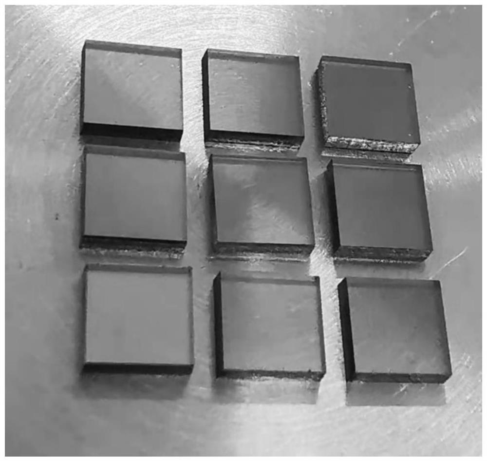
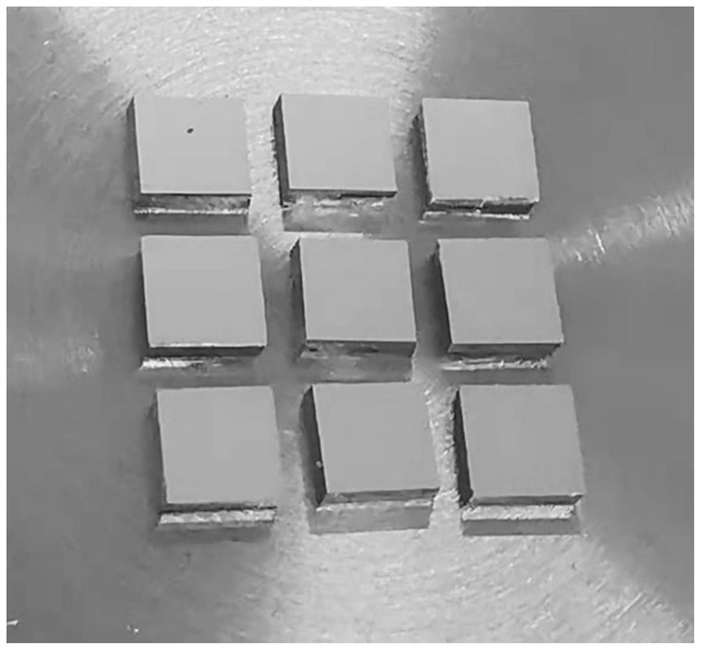
[0012] Specific embodiment one: the welding method of the single crystal diamond seed crystal and the sample holder in this embodiment is implemented according to the following steps:

[0013] 1. Surface pretreatment: Place multiple single crystal diamond seed crystals that have been ultrasonically cleaned with the bottom facing up on the substrate of the plasma cleaning machine, and then perform surface pretreatment with oxygen plasma to obtain pretreated single crystal diamond seed crystals;

[0014] 2. Coating: Place a plurality of pretreated single crystal diamond seeds on the coating substrate, with the surface treated by oxygen plasma facing up, and put it into the magnetron sputtering coating equipment, and select gold (purity is 99.99%) As a target material, a gold layer is then plated on the surface of the single crystal diamond seed crystal to obtain the coated single crystal diamond seed crystal;

[0015] 3. In-situ welding: Place multiple coated single crystal diam...

specific Embodiment approach 2

[0017] Embodiment 2: This embodiment differs from Embodiment 1 in that the distance between adjacent single crystal diamond seed crystals in step 1 is 0.5-2 mm.

[0018] The distance between the single crystal diamond seed crystals in this embodiment ensures that the seed crystals do not interfere with each other during the plasma pretreatment and increases the number of placements for one treatment.

specific Embodiment approach 3

[0019] Embodiment 3: The difference between this embodiment and Embodiment 1 or 2 is that in step 1, oxygen plasma surface pretreatment is carried out under the conditions of oxygen flow rate of 30 sccm, power of 600 W, and air pressure of 1 kPa.


PUM

PropertyMeasurementUnit
Thicknessaaaaaaaaaa

Abstract

The invention discloses a single crystal diamond seed crystal and sample holder welding method, and aims to solve the problems of seed crystal drifting and poor heat conduction in the growth process of CVD single crystal diamond. The welding method comprises the steps that 1, a plurality of monocrystal diamond seed crystals subjected to ultrasonic cleaning are placed on a substrate of a plasma cleaning machine with the bottoms face upwards, and then oxygen plasma surface pretreatment is conducted; 2, the surface of the monocrystal diamond seed crystal is plated with a gold layer by adopting magnetron sputtering coating equipment; and 3, the coated single crystal diamond seed crystal and a sample holder are put into MPCVD diamond growth equipment together, the interior of a growth cabin is vacuumized, and in-situ welding is performed when the air pressure in the growth cabin reaches 200-250 Torr, the microwave input power reaches 2500-3500 W and the temperature of the coated single crystal diamond seed crystal reaches 950-1050 DEG C. A plurality of seed crystals can be rapidly welded at a time, a connecting layer is uniform, connection is firm, and the cooling effect is improved.

Description

technical field [0001] The invention belongs to the field of material welding, and in particular relates to a seed crystal and sample holder welding method for homoepitaxial growth of single crystal diamond by microwave plasma chemical vapor deposition (MPCVD). Background technique [0002] Single crystal diamond is a simple form of carbon, which has a series of excellent material properties such as ultra-high hardness, ultra-high thermal conductivity, stable chemical properties, good insulation, and good transmittance. It has broad application prospects in aerospace, third-generation semiconductors, precision machining, optical windows and other fields. However, natural single crystal diamond is rare and its quality and size cannot meet the requirements of industrial applications. Synthetic diamond technology has become a hot research direction. Among them, microwave plasma chemical vapor deposition (MPCVD) is a rapid preparation technology of large-size, high-quality sing...

Claims


Application Information

Patent Timeline
IPC IPC(8): C30B29/04C30B25/20C23C14/35C23C14/18C23C14/02
CPCC30B29/04C30B25/186C30B25/205C23C14/35C23C14/185C23C14/022
Inventor 朱嘉琦李一村代兵郝晓斌文东岳赵继文张森
Owner HARBIN INST OF TECH
Features
  • R&D
  • Intellectual Property
  • Life Sciences
  • Materials
  • Tech Scout
  • Unparalleled Data Quality
  • Higher Quality Content
  • 60% Fewer Hallucinations
Learn More